


:quality(80)/p7i.vogel.de/wcms/99/dd/99dd64ae87c0855129bd405f61d81f81/0133290217v2.jpeg "Microchip’s new 1.2 V SY757xx clock buffers connect modern low-voltage SoCs, FPGAs and AI accelerators with higher-voltage clock components, supporting frequencies up to 250 MHz and additive jitter as low as 26 fs. (Source: Microchip)")
:quality(80)/p7i.vogel.de/wcms/83/d0/83d0b8ea52378c77f98358e29ceccfc0/0133339307v2.jpeg "Capacitors are a critical yet often overlooked component in AI data center power supplies, buffering energy and stabilizing voltage as racks scale toward the megawatt range. (Source: © Parilov - stock.adobe.com)")
:quality(80)/p7i.vogel.de/wcms/10/fc/10fcb98e44d61826e641bc8d3f20f616/0133193677v2.jpeg "The new AEVA and AEVB Series aluminum electrolytic capacitors are engineered for harsh industrial environments, delivering high-CV, long-lifetime performance in compact, surface-mount packages that reliably withstand up to 30g acceleration and operating temperatures extending from -55° to +125°C. (Source: Kyocera)")
:quality(80)/p7i.vogel.de/wcms/f7/42/f74208db9f5f87dca384b38b71c4782e/0133196365v2.jpeg "YAGEO’s EC Flat‑Series temperature sensors combine fast, accurate measurement with resistance to vibration, shock, moisture and dust for demanding automotive and industrial applications. (Source: Yageo)")
:quality(80)/p7i.vogel.de/wcms/57/b6/57b6d33cb929fa4408ad56803ed5f0bc/0133311998v2.jpeg "Elmos and SK keyfoundry are expanding their collaboration on 130 nm technology and have agreed on long-term wafer capacity through 2037 to support reliable automotive semiconductor production. (Source: © remake - stock.adobe.com)")
:quality(80)/p7i.vogel.de/wcms/b4/0a/b40a1de3c8fa631b2aff74ec436c43db/0133314066v2.jpeg "ZF Aftermarket expands its EV service portfolio with new repair kits and solutions for e‑motors, inverters, hybrid modules, mechatronics and electric drive units. (Source: ZF Aftermarket)")
:quality(80)/p7i.vogel.de/wcms/48/e1/48e107b92f976652532facf5ca1e0855/0133290826v2.jpeg "Infineon and SolarEdge are extending their collaboration to develop solid-state protection solutions for 800 VDC AI data centers, aiming to improve fault response, system reliability and power density. (Source: © Grispb - stock.adobe.com)")
:quality(80)/p7i.vogel.de/wcms/99/84/9984f5888ecc71c249f65cea3f0658d1/0133069650v2.jpeg "Yokogawa’s integrated measurement setup helps Vertiv analyse AI-driven pulsed loads, combining power, waveform and thermal data to validate UPS performance and input power smoothing. (Source: YOKOGAWA)")
:quality(80)/p7i.vogel.de/wcms/a4/29/a429b944eb0a69e268015f8300ba8940/0133311989v2.jpeg "Hitachi Energy and Daikin are establishing a German supply of C4‑FN, a specialty insulating gas used in SF₆‑free high‑voltage equipment for more sustainable power grids. (Source: © Ahmed - stock.adobe.com)")
:quality(80)/p7i.vogel.de/wcms/d5/32/d5326e4b05d5cd759e88062f1c0b097a/0133344193v2.jpeg "Co-packaged optics is the latest innovation in data centers where optical modules on silicon chips can assist in scaling megawatt AI infrastructure. (Source: © Rachakrit - stock.adobe.com)")
:quality(80)/p7i.vogel.de/wcms/76/a9/76a9333bc7c6abbf7e29d1b910edb5e2/0133335959v2.jpeg "This article explains PMBus in data center power supplies. (Source: © Gibster - stock.adobe.com)")
:quality(80)/p7i.vogel.de/wcms/35/9c/359cfb6c855204e4d114f88cf5b98b5f/0133078984v2.jpeg "Photonic integrated circuits are next-level chips that will dominate data centers in the upcoming years. (Source: © pier - stock.adobe.com)")
:quality(80)/p7i.vogel.de/wcms/7b/76/7b76005554b556df2a7a3794bdf69d44/0132365246v2.jpeg "Hioki’s ST5680A DC Hipot Tester combines CE/UKCA/CSA compliance, an integrated capacitance‑based contact check and time‑series waveform recording (voltage, leakage current, insulation resistance) to standardize hipot and insulation testing across EV cell, module and pack production lines. (Source: Hioki)")
:quality(80)/p7i.vogel.de/wcms/af/7f/af7f7b0fb7f29219fc991b1130f65477/0132241333v2.jpeg "Comprehensive laboratory testing regimens—combining thermal cycling, high‑current stress, EMC, and accelerated lifetime tests—are essential to validate advanced power designs and ensure reliability in real‑world applications. (Source: PRBX)")
:quality(80)/p7i.vogel.de/wcms/16/3d/163df69363f8125315a9826e13ea4b05/0131927425v2.jpeg "Solution will maximize data center and AI factory profitability while delivering engineering-grade insights to design and operations for more efficient, sustainable, and resilient infrastructure. (Source: Cadence)")
:quality(80)/p7i.vogel.de/wcms/85/b7/85b7e90733a2bd8f21515d8f7137f2fc/0131917677v2.jpeg "Renesas acquires Pictorus to integrate its embedded application software platform with Renesas’ MCU and MPU portfolio, helping developers shorten time‑to‑market and simplify system integration. (Source: © lucadp - stock.adobe.com)")
ENERGY HARVESTING Step-by-step mathematical dimensioning for energy harvesting power stages
Related Vendors
:fill(fff,0)/p7i.vogel.de/companies/6a/20/6a202a4f89a62/mrs-white-on-blue-bg.png "mrs-white-on-blue-bg ()")
:fill(fff,0)/p7i.vogel.de/companies/5f/71/5f71d5f92a5f6/2000px-rogers-corporation-logo-svg.png "2000px-Rogers_Corporation_Logo.svg.png (rogers germany)")
:fill(fff,0)/p7i.vogel.de/companies/68/2c/682c3e2e9a195/logotype-rvb.jpeg "logotype-rvb (MERSEN France)")
This article delivers a step-by-step mathematical framework to size components in ultra-low-power conversion stages, covering specific equations for dynamic impedance matching and quiescent current loss budgeting. This practical approach aims to guarantee system startup and long-term autonomy in battery-free IoT devices.

The proliferation of battery-free industrial IoT nodes and smart edge devices has accelerated the demand for micro-energy harvesting systems. However, bridging the gap between ambient energy sources—such as thermal gradients or indoor light—and a stable regulated voltage rail presents severe power electronics challenges. Transducers often output unpredictable, millivolt-range voltages, meaning that the success of the system relies entirely on a power conversion stage designed with meticulous efficiency and sub-microamp current management.
To overcome these constraints, hardware engineers cannot rely on trial-and-error prototyping; they require a rigorous analytical approach to component dimensioning. This article provides a step-by-step mathematical framework to accurately calculate storage elements, manage discontinuous conduction modes (DCM), and optimize dynamic impedance matching. By implementing these precise power budgeting calculations, designers can drastically minimize quiescent losses, guarantee system start-up under worst-case source conditions, and ensure true long-term autonomy.
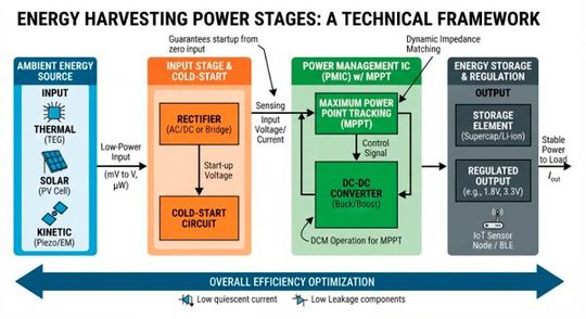
Source characterization: Modeling Rs and Voc
To design an efficient power conversion stage, the indispensable first step is the electrical modeling of the energy harvesting transducer. Because ambient energy sources are highly non-linear and critically dependent on environmental conditions, we must characterize their behavior using their Open-Circuit Voltage (Voc) and Internal Source Resistance (Rs). The analytical models for the three most common transducers are detailed below:
1. Thermoelectric Generators (TEG)
A TEG converts a direct temperature gradient into electrical energy via the Seebeck effect. From an electrical standpoint, a TEG behaves linearly and is ideally modeled as a DC voltage source in series with an internal resistance.
- Open-Circuit Voltage (Voc): It is directly proportional to the temperature differential between the hot (Th) and cold (Tc) plates of the device:
Where αpn is the Seebeck coefficient of a single thermoelectric couple, N is the number of series-connected couples, and αTEG is the global module coefficient.
- Internal Resistance (Rs): It depends primarily on the electrical resistivity of the semiconductor materials used (p-type and n-type) and the geometry of the pellets:
Where ⍴ represents resistivity, L is length, A is the cross-sectional area of the pellets, and Rcontact accounts for the metallic interconnect resistance losses.
2. Photovoltaic Transducers (Indoor/Outdoor Solar Cells)
Unlike TEGs, a photovoltaic cell is inherently non-linear and is modeled using the single-diode equivalent circuit.
- Open-Circuit Voltage (VOC): This occurs when the output current is zero, and it scales logarithmically with light irradiance (Iph):
Where n is the diode ideality factor, Vt = kB . T/q is the thermal voltage (≅ 26 mV at 25ºC), Iph is the photo-generated current (proportional to light), and I0 is the diode reverse saturation current.
- Equivalent Internal Resistance (RS): At the Maximum Power Point (MPP), the dynamic or equivalent internal resistance of the cell can be approximated by evaluating the derivative of the I-V curve:
For power stage design, RS_PV is not a constant value; it decreases inversely proportional to the ambient light levels.
3. Piezoelectric Transducers (Kinetic/Vibrational Energy)
Piezoelectric elements generate electric charge when subjected to mechanical strain. Since they operate under sinusoidal vibrations, they are modeled in the AC domain as a current source in parallel with an internal capacitance (CP) and a massive parasitic bulk leakage resistance (RP).
- Open-Circuit Voltage (VOC): Under open-circuit conditions, the generated AC voltage amplitude is directly linked to the mechanical displacement (x) and the piezoelectric properties:
Where d31 is the piezoelectric strain constant, Y is Young's modulus, and b, h, L are the physical dimensions of the cantilever beam.
- Internal Source Impedance (ZS): Because the capacitive nature of the material dominates at typical industrial vibration frequencies (10 Hz - 200 Hz), the internal resistance is treated as a frequency-dependent reactance governed by the excitation frequency (⍵):
Where Cp is typically in the nanofarad (nF) range, resulting in very high source impedances (kΩ to MΩ), requiring power stages with ultra-high input impedance.
:quality(80)/p7i.vogel.de/wcms/47/e1/47e15fce96f9a6bbc8e0e26c6723fc2f/0131803702v5.jpeg "Sustainable architecture: Advanced photovoltaic solar glass (Source: © Jo-El - stock.adobe.com)")
ELECTRONIC SYSTEMS
Solar, thermal, or piezo? Choosing the right power electronics for different energy harvesting sources
Impedance matching equations and dynamic MPPT
Once the transducers are properly characterized, the primary challenge of the power stage is to extract the maximum available power (Pmax). According to the Maximum Power Transfer Theorem, this condition is met when the input impedance seen by the power stage (Zin) matches the complex conjugate of the source impedance (Zs*). Since these energy harvesting sources operate either in DC or at very low vibration frequencies, this task simplifies to an equivalent resistance matching.
1. The Maximum Power Transfer Criterion (DC)
For resistive sources such as TEGs or linearized photovoltaic systems, the power transferred into the converter's input can be expressed mathematically
To find the optimal operating point, we take the derivative of the input power with respect to the converter's input resistance and set it to zero (dPin/dRin = 0), yielding the fundamental matching condition:
2. Resistance Emulation via Switching Converters in DCM
In ultra-low-power harvesters, running continuous microcontroller-driven MPPT routines consumes too much overhead energy. Instead, hardware designers leverage DC-DC converters (typically Boost or Buck-Boost topologies) operating in Discontinuous Conduction Mode (DCM).
In DCM, the average input current of the converter is directly proportional to the input voltage, meaning the switching network inherently behaves as an emulated resistor (Rin_DCM). For a Boost converter, this equivalent input resistance is governed by the following analytical equation:
Where L is the power stage inductance, D is the switching duty cycle, and TS is the switching period (1/fsw).
To achieve passive, sensorless MPPT, we equate the emulated resistance to the internal source resistance (Rin_DCM = RS), deriving the explicit design equation for the duty cycle:
3. Fractional Open-Circuit Voltage Algorithms (Fractional Voc)
For photovoltaic and thermoelectric transducers, the ratio between the voltage at the maximum power point (VMPP) and the open-circuit voltage (VOC) remains remarkably constant across changing environmental conditions. This allows the use of the Fractional VOC technique, described by the linear equation:
- For TEGs: The matching is perfectly symmetrical, making the proportionality factor exactly k = 0.5.
- For Photovoltaic (PV) Cells: Due to the diode physics, the optimal point shifts slightly higher, typically sitting within the range of k ∈ [0.7, 0.8].
The power stage controller periodically disconnects the transducer for a few milliseconds to sample and store VOC onto a holding capacitor, subsequently regulating the operating input voltage (Vin) to satisfy the equation above using an ultra-low-power analog control loop.
:quality(80)/p7i.vogel.de/wcms/3c/a1/3ca1e2527a00068eb37f1db220c5463a/0132042920v2.jpeg "Energy harvesting removes the need for periodic battery swaps in hard‑to‑reach sensors — economically and regulatorily attractive as EU battery rules raise compliance and lifecycle costs. (Source: © Plaifah - stock.adobe.com)")
SUSTAINABILITY
The end of battery obsolescence: energy harvesting as the backbone of green electronics
Inductor and capacitor selection in DCM
The physical dimensioning of magnetic and storage elements forms the core hardware of the power stage design. In micro-energy harvesting, these components do not merely define voltage and current ripple; they dictate whether the converter strictly operates in Discontinuous Conduction Mode (DCM), which is vital for maintaining the passive resistor emulation and sensorless MPPT derived in previous sections.
1. Engineering the Inductor (L)
To ensure that the converter operates strictly within the DCM boundaries across all input source conditions, the inductor current must return to zero before the end of the switching period (TS). The critical boundary condition for a Boost converter is governed by the dimensionless conduction parameter (K), which must satisfy the inequality:
From this boundary constraint, and knowing the design duty cycle (D) and switching frequency (fSW = 1/TS), we calculate the absolute maximum allowable value for the inductor using the following equation:
- Critical Parasitic Losses: Meeting the nominal inductance value is not enough. In ultra-low-power systems, the inductor's Direct Current Resistance (DCR) introduces significant Joule conduction losses (Irms2 . DCR) that can quickly destroy system efficiency. Designers must select inductors featuring ultra-low DCR (typically < 500 mΩ) and low-hysteresis magnetic core materials.
2. Dimensioning the Input Capacitor (Cin)
The input capacitor decouples the high-frequency current pulsations caused by the converter's switching network, keeping the transducer's operating voltage ripple close to a stable DC value near the MPP. The calculation of its minimum required capacitance is based on the acceptable peak-to-peak input voltage ripple (ΔVin), usually constrained to 1% or 2% of Vin:
- Leakage Current Criterion: The most critical selection parameter for Cin is its Direct Leakage Current. Standard electrolytic capacitors are strictly prohibited because their micro-ampere leakage currents can easily exceed the total power generated by the ambient transducer. Multi-layer ceramic capacitors (MLCCs) with X7R or X5R dielectrics and insulation resistances higher than 10 GΩ must be utilized.
3. Sizing the Output / Storage Capacitor (Cout)
Since ambient energy harvesting is inherently intermittent, the output capacitor often serves as a short-term energy buffer (either a supercapacitor or a massive MLCC array). Assuming a constant-current discharge stage (Iload) drawn by the load during active application events (e.g., an MCU transmitting RF data packets), the minimum capacitance is calculated based on the burst duration (tburst) and the maximum allowed voltage drop (ΔVout = Vmax - Vmin):
To prevent power budget drain during long intervals when the system is in deep sleep, supercapacitors must be specified with minimal Equivalent Series Resistance (ESR) and self-discharge rates well below one micro-ampere.
:quality(80)/p7i.vogel.de/wcms/14/cb/14cb5de653f1cd959cd73991651da34c/0132042004v2.jpeg "Energy harvesting succeeds or fails at the PMIC level — from cold‑start circuits and nanopower quiescent currents to MPPT and buffer management, power electronics determine whether microwatt sources can sustain real devices. (Source: © Johnnii - stock.adobe.com)")
BASIC KNOWLEDGE
Energy harvesting: how it works, and why power electronics decide whether it's viable
Efficiency budgeting and loss modeling
The ultimate success in sizing a power conversion stage for energy harvesting is not measured merely by its voltage regulation capability, but by its net energy balance. In systems operating within microwatt (μW) power budgets, the total parasitic loss (Ploss) must be strictly lower than the maximum power extracted from the source (Pin). The analytical breakdown of the switching converter's efficiency budget is governed by the following general equation:
1. Conduction Losses (P conduction)
Since the converter operates in DCM, the peak inductor current (Ipk) is significantly higher than the average current. Conduction losses across the MOSFET's on-resistance (RDS(on)) and the inductor's direct current resistance (DCR) are computed using the root-mean-square current (Irms):
2. Switching and Dynamic Losses (P switching + P magnetic)
Every switching cycle drains energy due to the charging and discharging of the MOSFET's parasitic output capacitance (Coss) and the gate charge (Qg). At higher switching frequencies (fsw), these losses dominate the power stage overhead:
Magnetic losses (Pmagnetic) account for the inductor core losses due to hysteresis and eddy currents, which are dependent on the specific core material selection.
3. Static Quiescent Current Losses (P static)
During light-load states or when the system is waiting in standby for the storage buffer to accumulate enough energy, the quiescent current (Iq or house-keeping current) of the control IC becomes the primary efficiency killer:
To ensure system viability, designers must specify control ICs or design analog control loops with sub-microampere quiescent currents (typically < 500 nA).
Conclusions
Designing power electronics for micro-energy harvesting applications requires abandoning the traditional approximations and empirical rules utilized in conventional higher-power conversion. By implementing the mathematical framework detailed in this article, hardware design engineers can:
- Guarantee Reliable Cold-Start: Ensuring that the transducer's open-circuit voltage and baseline power output comfortably overcome the critical hardware wake-up thresholds.
- Maximize Passive Extraction: Exploiting the natural resistive emulation of the DCM switching network to achieve optimal impedance matching without the power overhead of complex digital MPPT loops.
- Extend System Lifespan: Specifying low-DCR inductors and high-insulation ceramic capacitors eliminates the reliance on chemical batteries entirely, enabling the deployment of truly autonomous, maintenance-free industrial IoT nodes that can operate reliably for decades.
(ID:50904779)
:quality(80)/p7i.vogel.de/wcms/5c/f5/5cf53b6db2706b86ac6eb5c407704d27/0131699647v2.jpeg "This article explains inductors in electrical and electronics engineering. (Source: © Iurii - stock.adobe.com)")
:quality(80)/p7i.vogel.de/wcms/aa/a3/aaa3c94040c99a7aafb263e839b9ab22/0130953280v2.jpeg "The negative resistance effect can be verified in non-linear or non-ohmic devices, including many semiconductor devices, which are applicable in the power and RF industries. (Source: © ruangrit19 - stock.adobe.com)")