

















HIGH FREQUENCY POWER Hard switching vs. soft switching in high-frequency power converters
One of the main methods to decrease the size of power converters is increasing switching frequency. Higher frequency can reduce the required values of inductors and capacitors, leading to more compact designs with higher power density. But faster switching also makes the losses in turn-on and turn-off of power devices more important.

Generally there are two methods to manage the losses, namely hard switching and soft switching. A relatively simple realization makes hard switching widely used. Soft switching techniques include zero voltage switching (ZVS) and zero current switching (ZCS). The philosophy of these methods is to regulate voltage or current at the switching transition to reduce switching losses.
Neither way is always the best. The optimal choice depends on the converter topology, operating frequency, load range, semiconductor characteristics, and overall system requirements.
The article discusses the major differences between hard switching and soft switching, the loss mechanisms involved, and the practical issues in choosing a switching scheme. The reference books listed at the end of this article are recommended for further reading. [1] [2]
Power by Maurizio
About the author

Maurizio Di Paolo Emilio is a physicist, engineer, and technical author with a passion for technology and innovation. Curious by nature, he explores how technology works, how it evolves, and where it is heading.
Why switching losses become critical
An ideal switch alternates instantaneously between two states: fully on, with negligible voltage across it, and fully off, with negligible current flowing through it. Real semiconductor devices require finite time to transition between these states. During a switching transition, voltage and current may overlap. The instantaneous power dissipated by a transistor can be expressed as:
where vds(t) is the drain-to-source voltage and id(t) is the drain current. The energy associated with a switching transition can be calculated by integrating the instantaneous terminal power over the relevant interval. When evaluating the energy dissipated within the semiconductor, the contribution of energy stored in or released from device capacitances must also be considered:
If this E represents the combined energy dissipated during turn-on and turn-off in one complete switching cycle, the corresponding average switching power is approximately
where fs is the switching frequency.
This relationship explains why switching losses can become a major limitation at high frequencies: even if the energy dissipated per cycle remains constant, the average switching loss increases with frequency. In practice, the energy per cycle may also change with operating conditions.
Switching loss is only a portion of the total loss budget. Also to be taken into account are conduction losses, gate-drive losses, magnetic losses, and losses associated with parasitic elements. Thus, the goal is not just to minimize switching energy but to minimize total system losses subject to the required electrical and thermal constraints.
Hard switching: Simplicity and its limitations
In hard switching, the control circuit forces the transistor to turn ON or OFF while the voltage across the device and the current flowing through it may be non-zero. This leads to a voltage-current overlap period during the switching transition, which results in energy dissipation in the semiconductor device.
In addition, since switching energy is dissipated at each switching cycle, higher switching frequencies generally result in higher average switching losses. As the frequency increases, thermal management becomes more challenging, which may limit the converter efficiency and power density.
Hard switching can also generate electromagnetic interference (EMI) due to high rates of change of voltage (dv/dt) and current (di/dt). Parasitic inductances and capacitances may produce voltage overshoots and ringing, while reverse-recovery effects can increase current peaks and switching losses. The rates of change of voltage and current must therefore be balanced against switching losses and EMI requirements: faster transitions can reduce switching losses but may increase electromagnetic emissions. In severe cases, these transients may push the device beyond its voltage or current ratings or its safe operating area (SOA).
In MOSFETs, turn-on losses can be caused by the voltage-current overlap but also by the energy lost during the discharge of the output capacitance through the conducting device. The relative importance of these mechanisms depends on the device, the circuit topology, and the operating conditions.
In circuits with MOSFET body diodes, reverse recovery can also impact switching losses and current stresses. Its impact depends on the device technology and commutation conditions; it should not be assumed negligible just because a converter uses a soft-switching technique.
Nevertheless, hard switching is still widely used due to its relatively simple circuit implementation and control. Its applicability is determined by the switching frequency, semiconductor characteristics, layout, gate-drive design, and the capacity to control switching losses and electrical stress.
Snubbers and damping networks can aid in limiting voltage overshoot and ringing, but dissipative implementations add additional losses. Another technique to reduce the switching stress is soft switching, where the waveform of the voltage or the current is controlled during the transition, but this requires extra components and more complex timing. [3]
Soft switching: ZVS, ZCS
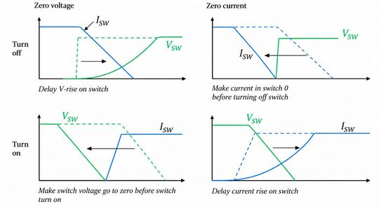
Soft switching minimizes switching losses by controlling the voltage and current waveforms during semiconductor transitions. In hard switching, voltage and current can be simultaneously high. Soft-switching techniques create conditions that minimize voltage/current overlap during turn-on or turn-off.
The two basic approaches are zero voltage switching (ZVS) and zero current switching (ZCS). In ZVS the voltage across the switch is made to approach zero at switching time and ZCS reduces the current through the device. These conditions can be achieved by means of resonant circuit elements, controlled commutation intervals, or auxiliary switching networks.
Zero-voltage switching (ZVS)
Zero voltage switching is a method in which the voltage across the semiconductor is brought close to zero before the device is turned on. This reduces the overlap of drain-to-source voltage and drain current during turn-on and thus the energy dissipated in the switching transition.
In MOSFET converters, ZVS is normally achieved by discharging the device's output capacitance before the channel starts conducting. In many topologies, the energy stored in inductive elements is used to charge/discharge the output capacitances of the switches during a commutation interval. Depending on the device technology, current may temporarily flow through the body diode of a silicon MOSFET or through the reverse-conduction mechanism of a GaN HEMT before the gate is driven on.
This mechanism is of particular interest at high switching frequencies where losses associated with the output capacitance may become a significant portion of the total loss budget. ZVS can substantially reduce the capacitive energy dissipated during the transition by reducing the drain-to-source voltage to nearly zero prior to turn-on.
However, ZVS requires sufficient commutation current and proper timing. The available energy and commutation time must be sufficient to discharge the output capacitance of the device about to turn on, bringing its drain-to-source voltage close to zero before gate activation. If the available current or transition time is insufficient, the device may turn on with a residual voltage across it, resulting in partial or complete loss of ZVS.
This restriction can be of particular importance at light load, when the energy available for charging and discharging the device's capacitances may decrease. Therefore, some converter topologies require additional control strategies or circulating current to achieve ZVS over a wide operating range.
ZVS on turn-on does not ensure low losses on turn-off, either. Gate-drive losses and other parasitic effects can still be substantial depending on the topology and the voltage-current overlap. Turn-off transitions can be shaped to reduce voltage-current overlap. However, the mechanisms and operating conditions are different than the ones used for turn-on ZVS.
Zero current switching (ZCS) method
Zero-current switching decreases switching losses by forcing the current through the semiconductor to be close to zero at the instant of switching. The ZCS is particularly beneficial during turn-off, because the reduction of the current before the device stops conducting reduces the voltage-current overlap and can minimize the switching stress caused by parasitic inductances.
ZCS can also be achieved at turn-on by controlling the rise of current during the transition. In all cases, the goal is to avoid switching when a large voltage and current are simultaneously present across and through the device.
Resonant converters use inductors and capacitors to shape the current waveform such that switching occurs near a natural current zero. For example, a series-resonant path can offer the current conditions for ZCS. However, the detailed implementation depends on the converter topology, and the existence of a resonant network does not guarantee the zero-current switching.
A major limitation of ZCS is that reducing the switching current does not necessarily eliminate losses associated with semiconductor output capacitance. If the MOSFET is turned on with a large voltage across drain and source, the energy stored in the output capacitance can still be dissipated during the transition.
Thus, ZCS can reduce current-dependent switching losses, while voltage-dependent loss mechanisms, including those associated with output capacitance, may remain significant. Ringing or voltage overshoot can also be caused by parasitic capacitances and inductances even when the current is near zero at the switching instant.
Soft switch is not a lossless switch
While ZVS and ZCS may substantially decrease switching losses, neither technique guarantees lossless operation. In practice, the switching transitions may be only partially softened, and the semiconductor may still experience residual voltage-current overlap, conduction losses, gate-drive losses, and losses due to parasitic elements.
Moreover, the soft-switching conditions are not guaranteed for the whole operating range. Changes in input voltage, load current, switching frequency, and component tolerances can affect the resonant transition and the energy available for commutation.
Achieving soft switching may require additional components, more complex control strategies, or increased circulating current. These factors can introduce additional conduction losses and electrical stresses that partially offset the reduction in switching losses.
Finally, soft switching does not eliminate electromagnetic interference or guarantee operation within the safe operating area (SOA) of the semiconductor. Voltage overshoot, ringing, peak currents, and transient conditions need to be considered by proper circuit analysis, simulation, and experimental measurements.
The trade-off: Switching losses vs. conduction losses
The main problem in designing soft-switching circuits is finding the right trade-off between reduced switching losses and increased conduction losses, device stress, and extra circuitry.
In resonant converters, inductors and capacitors are used to shape switching transitions. This can reduce the switching losses but energy is circulated between the reactive elements during the switching cycle. The resulting current may be larger than the current needed to transfer useful power to the load, increasing conduction losses.
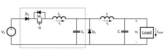
This trade-off is illustrated by a zero-current-switching quasi-resonant buck converter. The advantages are smooth switching transitions and low switching losses at moderate frequencies. However, the resonant action and the circulating energy in the circuit can cause higher conduction losses than a conventional PWM converter. Higher diode voltage requirements and the need to control the switching frequency over a wide range can also complicate the design.
In ZVS converters, maintaining soft-switching conditions at light load can be challenging due to reduced commutation current and available inductive energy. Additional control strategies may be required, introducing further design trade-offs.
Reduced switching overlap does not guarantee safe operation. Voltage overshoot, ringing, and transient current peaks can still exceed device ratings, requiring careful evaluation of electrical stress and operating limits.
The relevant comparison is therefore not hard switching versus soft switching. The total loss over the expected range of operation of the converter, including various loads and input voltages, is considered.
Practical example: ZCS quasi-resonant buck converter
Soft switching can be implemented by using resonant components to control the voltage and current transitions of the semiconductor devices.
A ZCS quasi-resonant buck converter uses resonant inductance and capacitance to shape the switching current, allowing the main switch to operate under zero-current switching conditions. In the topology illustrated in Figure 2, the resonant inductor limits the current rise when the main switch turns on. The resonant capacitor then participates in the subsequent resonant transition, allowing the switch current to return to zero before turn-off. This approach can reduce switching losses and produce smoother switching waveforms.
However, the resonant action introduces circulating energy, which can increase conduction losses compared with a conventional PWM converter. Other limitations include increased peak voltage and current stresses, possible voltage ringing, increased diode voltage requirements, and a wide switching-frequency range for output regulation.
Choosing the right approach
The choice of hard switching versus soft switching must be made considering the entire system of the converter, not only considering the switching losses. The switching frequency is an important starting point, because hard switching losses can become increasingly significant at higher frequencies. However, the efficiency must be assessed over the expected working range from light load to full load, where the benefits of a particular switching strategy may change.
Furthermore, device properties are very important. Output-capacitance energy, reverse-recovery behavior, and other switching-related effects can affect overall losses and can help determine which approach is better suited. The chosen topology and control strategy should also be able to achieve the desired zero-voltage switching (ZVS) or zero-current switching (ZCS) conditions without adding unnecessary complexity or circulating currents.
Other considerations are thermal performance, voltage stress, and electromagnetic interference (EMI). The switching waveforms should be simulated and measured to verify that voltage and current are within the device ratings and safe operating area (SOA), including transient conditions. Beyond electrical performance, designers must assess if projected efficiency gains warrant the added components, control needs, and development effort, particularly if cost and power density are primary considerations.
In practice, hard switching may be preferred when ease of circuit design and operation over a wide range of conditions is of prime importance. The reduction of switching losses can improve the efficiency of the converter and allow greater power density. These advantages make soft switching especially attractive at higher switching frequencies, if the necessary switching conditions can be maintained.
GaN and SiC devices offer designers more flexibility, but neither technology eliminates these trade-offs. The best results still depend on the careful coordination of the semiconductor devices, the gate drive, the switching frequency, the magnetics, the PCB layout, and the control strategy.
Ultimately, the decision of whether to use hard or soft switching should be based on the actual operating requirements of the converter, not on an assumption that one approach is more efficient than the other. The ideal choice is the one that provides the correct trade-off between efficiency, reliability, power density, complexity, and cost for the designed operating conditions.
References
- 1. R. W. Erickson and D. Maksimović, Fundamentals of Power Electronics, 2nd ed., Springer, 2001. DOI: https://doi.org/10.1007/b100747. Relevant material: Chapter 4, “Switch Realization,” and Chapter 20, “Resonant Conversion.”
- 2. H.-P. Park, M. Kim, and J.-H. Jung, “A Comprehensive Overview in Control Algorithms for High Switching-Frequency LLC Resonant Converter,” Energies, vol. 13, no. 17, article 4455, 2020. https://doi.org/10.3390/en13174455
- 3. D. Perreault, “Soft-Switching 1,” Lecture 33, 6.622 Power Electronics, Massachusetts Institute of Technology (MIT), Spring 2023. MIT OpenCourseWare Lecture Slides.
- 4. Stanford University, “Soft Switching,” EE152: Power Electronics, lecture slides, October 26, 2015. Available online: https://web.stanford.edu/class/ee152/lecture_slides/Soft_Switching_102615.pdf
(ID:50993223)