nfineon Technologies AG is launching its OptiMOS 7 40 V switching-optimized power MOSFET portfolio for AI servers, data centers and telecom infrastructure. Designed for high-frequency DC-DC power conversion, the devices help designers improve efficiency and power density in space-constrained systems.
Infineon’s OptiMOS 7 40 V MOSFETs target high-frequency DC-DC conversion in AI servers, data centers and telecom infrastructure, including secondary-side stages in 800 V and 48 V power architectures.
(Bild: Infineon)
Target applications include low-voltage secondary-side stages of high-voltage intermediate bus converters in emerging 800 V DC architectures and intermediate bus converters in 48 V power architectures, with switching frequencies beyond 1 MHz supported in suitable topologies.
“With the OptiMOS 7 40 V, we give designers a MOSFET that cuts conduction and switching losses at the same time, so they can raise power density in the very limited space of an AI server,” said Richard Kuncic, Business Line Head Power Switches at Infineon. “It fits the secondary side of emerging 800 V DC architectures as well as today's 48 V designs, which lets our customers move to the next architecture at their own pace."
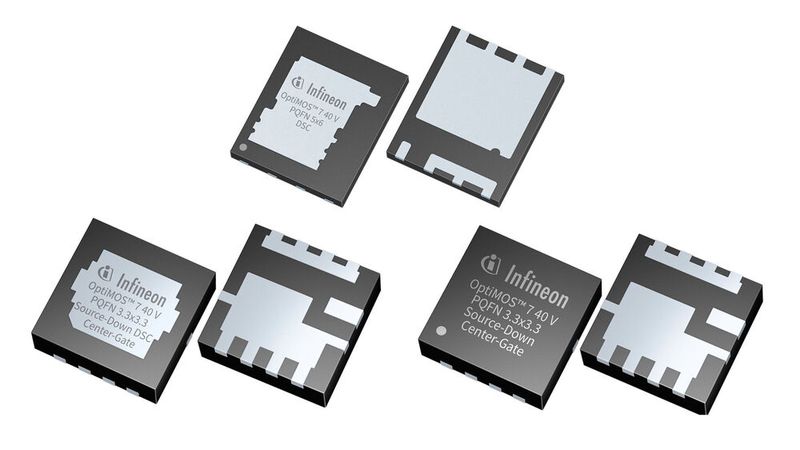
The OptiMOS 7 40 V portfolio balances on-state resistance (RDS(on)), output charge (Qoss) and gate charge (Qg) to address both conduction and switching losses. In a comparison of the source-down device IQE010N04LM7CGSC with its OptiMOS 6 predecessor IQE013N04LM6CGSC, maximum RDS(on) at a gate-source voltage of 4.5 V is reduced by up to 33 percent, while the figures of merit for output charge and gate charge are each reduced by up to 35 percent. Optimized for 5 V gate drive, the devices support gate-drive ecosystems used with GaN and are rated for junction temperatures up to 175 °C.
Source-down and dual-side cooling package options provide flexibility for compact layouts and thermal management. The IQE010N04LM7CG and IQE010N04LM7CGSC are offered in PQFN 3.3 mm × 3.3 mm source-down center gate packages, with overmolded and dual-side cooling options. Both feature a maximum RDS(on) of 1.0 mΩ at a gate-source voltage of 10 V. The portfolio also includes the ISCH65N04LM7SC, ISCH69N04LM7SC and ISC011N04LM7SC in PQFN 5 mm × 6 mm drain-down packages with dual-side cooling, featuring maximum RDS(on) values of 0.65 mΩ, 0.69 mΩ and 1.1 mΩ, respectively, at a gate-source voltage of 10 V.
Follow us on LinkedIn
Have you enjoyed reading this article? Then follow us on LinkedIn and stay up-to-date with daily posts about the latest developments on the industry, products and applications, tools and software as well as research and development.
It goes without saying that we treat your personal data responsibly. Where we collect personal data from you, we process the data in compliance with the relevant data protection regulations. More detailed information is available in our privacy policy.
Consent to the use of data for advertising purposes
I consent to the use of my email address to send editorial newsletters by Mesago Messe Frankfurt GmbH, Rotebühlstr. 83-85, 70178 Stuttgart, Germany including all of its affiliates within the meaning of Section 15 et seq. AktG (‘Mesago’). I have viewed lists of each group of affiliates here for the Mesago. The content of the newsletter covers the products and services of all of the companies listed above including, for example, trade magazines and specialist books, events and exhibitions and event-related products and services, printed and digital media products and services such as additional (editorial) newsletters, competitions, lead campaigns, online and offline market research, technical web portals and e-learning courses. If my personal telephone number has also been collected, it may be used to send offers for the aforementioned products and services from the above companies, as well as for market research purposes. If I wish to access protected content online on portals of Mesago including its affiliates within the meaning of Section 15 et seq. AktG, I must register with additional data in order to access that content. In return for this free access to editorial content, my data may be used in line with this declaration of consent for the purposes described herein.
Right to withdraw consent
I am aware that I can withdraw this consent at any time with future effect. My withdrawal of consent does not affect the lawfulness of processing performed based on my consent before its withdrawal. If I wish to withdraw my consent, I can send an email to Mesago at privacy@mesago.com. If I no longer wish to receive individual newsletters to which I have subscribed, I can also click on the unsubscribe link at the bottom of a newsletter. I can find more information on my right to withdraw, how to exercise this right and the consequences of my withdrawal in the Privacy policyEditorial newsletters section.