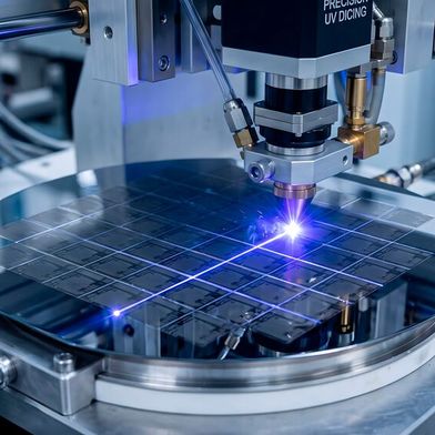
Infineon Technologies AG and Wolfspeed, Inc. have signed a new multi-year supply agreement for 200-millimeter silicon carbide (SiC) wafers, transitioning Infineon's existing Wolfspeed supply relationship from 150-millimeter to 200-millimeter substrate technology. SiC semiconductors have become a key enabling technology for the electrification and energy efficiency applications that drive global decarbonization, from electric vehicles and renewable energy systems to AI datacenter power infrastructure.
Multi-year agreement with Wolfspeed supports Infineon’s conversion from 150-millimeter to 200-millimeter silicon carbide (SiC) manufacturing
The agreement directly supports Infineon's conversion to 200-millimeter SiC manufacturing, strengthening Infineon's position as the global leader in power semiconductors and reinforcing the supply chain resilience that underpins its SiC growth strategy.
“Silicon carbide is at the heart of the energy transition, and securing a high-quality, resilient supply of 200-millimeter substrates is essential to delivering on our customers’ long-term commitments,” said Alexander Gorski, Chief Operations Officer at Infineon. “This agreement further broadens our strong supply base for our 200-millimeter high-volume manufacturing, building on a 20-year supply relationship between our two companies. It strengthens supply chain security for our customers and provides additional flexibility and scalability to support Infineon's future growth.”
AI datacenters are beginning to emerge as a significant demand driver for SiC power semiconductors. Power conversion efficiency across the datacenter power chain is a direct operating cost consideration for hyperscalers managing infrastructure at scale. The switching efficiency and thermal performance of SiC make it a technically suitable option for specific power conversion stages where silicon reaches its practical limits. Together with growing SiC adoption across electric vehicle drivetrains, solar inverters and industrial motor drives, these trends support a strong long-term outlook for high-quality 200-millimeter SiC substrates.
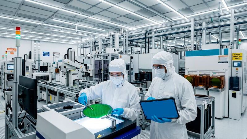
The transition to 200-millimeter SiC wafers delivers large manufacturing economics compared to 150-millimeter production. Larger wafer diameter increases usable die area per wafer, reduces per-unit substrate cost, and improves overall manufacturing efficiency. Infineon operates a multi-source SiC substrate strategy to maintain supply chain flexibility and quality across its global manufacturing network, including its world-class 200-millimeter SiC fab in Kulim, Malaysia, which is designed to be the world’s largest and most competitive silicon carbide manufacturing facility.
Follow us on LinkedIn
Have you enjoyed reading this article? Then follow us on LinkedIn and stay up-to-date with daily posts about the latest developments on the industry, products and applications, tools and software as well as research and development.
It goes without saying that we treat your personal data responsibly. Where we collect personal data from you, we process the data in compliance with the relevant data protection regulations. More detailed information is available in our privacy policy.
Consent to the use of data for advertising purposes
I consent to the use of my email address to send editorial newsletters by Mesago Messe Frankfurt GmbH, Rotebühlstr. 83-85, 70178 Stuttgart, Germany including all of its affiliates within the meaning of Section 15 et seq. AktG (‘Mesago’). I have viewed lists of each group of affiliates here for the Mesago. The content of the newsletter covers the products and services of all of the companies listed above including, for example, trade magazines and specialist books, events and exhibitions and event-related products and services, printed and digital media products and services such as additional (editorial) newsletters, competitions, lead campaigns, online and offline market research, technical web portals and e-learning courses. If my personal telephone number has also been collected, it may be used to send offers for the aforementioned products and services from the above companies, as well as for market research purposes. If I wish to access protected content online on portals of Mesago including its affiliates within the meaning of Section 15 et seq. AktG, I must register with additional data in order to access that content. In return for this free access to editorial content, my data may be used in line with this declaration of consent for the purposes described herein.
Right to withdraw consent
I am aware that I can withdraw this consent at any time with future effect. My withdrawal of consent does not affect the lawfulness of processing performed based on my consent before its withdrawal. If I wish to withdraw my consent, I can send an email to Mesago at privacy@mesago.com. If I no longer wish to receive individual newsletters to which I have subscribed, I can also click on the unsubscribe link at the bottom of a newsletter. I can find more information on my right to withdraw, how to exercise this right and the consequences of my withdrawal in the Privacy policyEditorial newsletters section.