


:quality(80)/p7i.vogel.de/wcms/7f/4b/7f4b97757cea82c0675209630577dc22/0133974130v2.jpeg "Vox Power’s EIRE600 delivers up to 600 W in a compact 5 × 3-inch package, with forced-air or conduction cooling options for industrial and medical equipment. (Source: Vox Power)")
:quality(80)/p7i.vogel.de/wcms/55/97/5597c3436e3bc92ee7ba23b6f9d289e9/0134032539v2.jpeg "Littelfuse’s TP7.0SMD-XC automotive TVS diode series uses foldback technology to provide low clamping voltage for protecting sensitive vehicle electronics. (Bild: Littelfuse)")
:quality(80)/p7i.vogel.de/wcms/51/f8/51f84448e666230bb11a02566abd1177/0133958187v3.jpeg "Microchip’s radiation-tolerant GaN point-of-load converter supplies up to 20 A for space-based processors, FPGAs, microcontrollers and ASICs. (Source: Microchip)")
:quality(80)/p7i.vogel.de/wcms/0a/7c/0a7c08f368ae1d91f758dd18d2a32e88/0133978423v2.jpeg "EPFL researchers have demonstrated a GaN transistor that withstands nearly 4 kV, using an intrinsic polarization superjunction design to distribute electric fields more evenly. (Source: EPFL)")
:quality(80)/p7i.vogel.de/wcms/5b/94/5b94232ca4183d6fcc2dccc7394d7544/0134041114v4.jpeg "Siemens and NVIDIA are testing AI applications at Siemens’ Erlangen electronics factory, using digital twins to support production planning and prepare inspection systems before physical prototypes are available. (Bild: Siemens)")
:quality(80)/p7i.vogel.de/wcms/b4/1f/b41f2731a07b608e60eca3663e280301/0133980549v2.jpeg "Multi-year agreement with Wolfspeed supports Infineon’s conversion from 150-millimeter to 200-millimeter silicon carbide (SiC) manufacturing (Source: © Ada - stock.adobe.com)")
:quality(80)/p7i.vogel.de/wcms/e3/0a/e30a8813bcf44b16f0dceb63a0747d29/0133984094v2.jpeg "The semiconductor is only one part of the design. Higher voltage, frequency and power density also increase the demands on electronic packaging materials such as die attach, substrates, top-side interconnects and module attach. (Source: Generated by AI)")
:quality(80)/p7i.vogel.de/wcms/5d/fb/5dfba5e5f38daf2b8597b05656af29c0/0133956337v2.jpeg "Wolfspeed has received a conditional commitment for a loan of up to $1.5 billion from the U.S. Department of War to support its domestic wide-bandgap semiconductor supply chain. (Source: © AspctStyle - stock.adobe.com)")
:quality(80)/p7i.vogel.de/wcms/bf/b6/bfb6ac295759be32d567df9849b6767e/0134094495v2.jpeg "Fraunhofer ISE reports that 25 Ah pouch cells with silicon-rich anodes retained more than 83% of their initial capacity after 1,000 cycles when tested under 1,000 kPa axial pressure. (Bild: Fraunhofer ISE)")
:quality(80)/p7i.vogel.de/wcms/16/dc/16dca55e6ef80e6b5da68bc628da2dcc/0133844782v2.jpeg "This article explains virtual power plants in modern renewable-heavy grids. (Source: © M@rketVisualsStudio - stock.adobe.com)")
:quality(80)/p7i.vogel.de/wcms/e8/33/e8330aae4bea3578b98ec2c1403d367a/0133980001v2.jpeg "IRENA’s 2026 World Energy Transition Outlook identifies faster electrification powered by renewables as central to meeting future global energy needs. (Source: Irena)")
:quality(80)/p7i.vogel.de/wcms/6c/b4/6cb405f47d25035e256ae90fe3a66ee6/0134032112v2.jpeg "Sungrow’s PowerTitan 3.0 energy storage platform uses onsemi EliteSiC hybrid power modules, with the companies reporting peak inverter efficiency above 99.3%. (Bild: onsemi)")
:quality(80)/p7i.vogel.de/wcms/7b/76/7b76005554b556df2a7a3794bdf69d44/0132365246v2.jpeg "Hioki’s ST5680A DC Hipot Tester combines CE/UKCA/CSA compliance, an integrated capacitance‑based contact check and time‑series waveform recording (voltage, leakage current, insulation resistance) to standardize hipot and insulation testing across EV cell, module and pack production lines. (Source: Hioki)")
:quality(80)/p7i.vogel.de/wcms/af/7f/af7f7b0fb7f29219fc991b1130f65477/0132241333v2.jpeg "Comprehensive laboratory testing regimens—combining thermal cycling, high‑current stress, EMC, and accelerated lifetime tests—are essential to validate advanced power designs and ensure reliability in real‑world applications. (Source: PRBX)")
:quality(80)/p7i.vogel.de/wcms/16/3d/163df69363f8125315a9826e13ea4b05/0131927425v2.jpeg "Solution will maximize data center and AI factory profitability while delivering engineering-grade insights to design and operations for more efficient, sustainable, and resilient infrastructure. (Source: Cadence)")
:quality(80)/p7i.vogel.de/wcms/85/b7/85b7e90733a2bd8f21515d8f7137f2fc/0131917677v2.jpeg "Renesas acquires Pictorus to integrate its embedded application software platform with Renesas’ MCU and MPU portfolio, helping developers shorten time‑to‑market and simplify system integration. (Source: © lucadp - stock.adobe.com)")
:quality(80)/p7i.vogel.de/wcms/f8/34/f834240d434a0c265a2ccafe614c8cd7/0134032109v4.jpeg "Hard- and soft-switching techniques shape voltage and current during device transitions, influencing switching losses, EMI and thermal performance in power converters. (Bild: © Mrthullab - stock.adobe.com)")
:quality(80)/p7i.vogel.de/wcms/27/07/2707280c807689b437baed3660257404/0133626052v2.jpeg "The quantum behavior of electrons shapes semiconductor devices—and the power converters that deliver electricity to modern computing systems. (Source: © Celt Studio - stock.adobe.com)")
:quality(80)/thumbor.vogel.de/mguFAwuAxCGw9kVi3c_k2-HNi5I=/500x500/p7i.vogel.de/wcms/66/74/667444027a724/tof1.jpeg "Christophe Basso")
AVERAGE MODELING Average models are versatile design companions
Related Vendors
:fill(fff,0)/p7i.vogel.de/companies/6a/20/6a202a4f89a62/mrs-white-on-blue-bg.png "mrs-white-on-blue-bg ()")
:fill(fff,0)/p7i.vogel.de/companies/63/d8/63d8d8a4c1ec0/mev-logo-rgb-s.jpeg "mev-logo-rgb-s (MEV Logo)")
Average models are available for many years to power supply designers using SPICE as a simulation engine. Considering the absence of switching component in the models, they simulate fast and are extremely useful to analyze dc-dc converters in the low- or high-voltage arena. Based on a set of nonlinear expressions, these models are linearized by SPICE around a dc operating point, making the models capable of predicting the small-signal response of a given converter such as a buck or a buck-boost type for example.

It is however less known that these models can be efficiently used in more complex environments such as three-phase power factor correction (PFC) in which they excel in simulation speed but also in ac analyses, crucial for stabilizing loops. This article will describe what average modeling implies and how designers can apply this concept for stabilizing PFC circuits.
Average modeling with state-space averaging
When analyzing the ac response of a switching converter, you need to describe the operating waveforms with time-continuous equations. One option is to resort to the state-space averaging technique (SSA) introduced in 1976 by Dr. Ćuk [1]. This technique requires the manipulation of matrixes describing the converter’s state variables for the two or three operational modes the circuit crosses while operating. A smoothing process is then applied to build a set of nonlinear but time-continuous expressions, later linearized to build an equivalent electrical model. With this linear model in hand, the designer can apply the Laplace transform and extract the transfer functions of his choice. One major drawback, in my opinion, lies in the fact that SSA considers the entire converter for modeling purposes. Should you want to add a parasitic term in the circuit to check its effect on the ac response, you would need to restart the analysis from scratch.
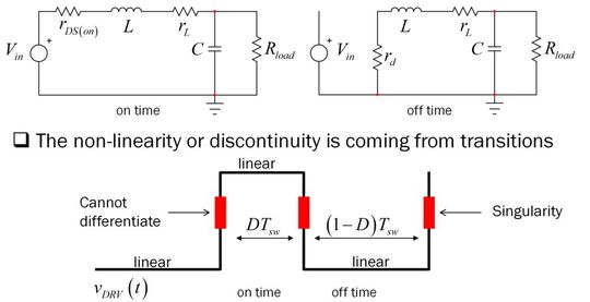
When the switch turns on, the input source biases the RLC network through the transistor’s rDS(on). When the main power switch is off, the same RLC network is involved, this time with the freewheel diode conducting. As explained in the previous lines, you need a link between these two distinct states for describing the circuit along a complete switching period. Unfortunately, a singularity occurs during the switch transitions from the on-to-off state and vice versa. The SSA provides a convenient way to smooth this discontinuity by observing that each linear network is active during DTSW (on-time) or (1-D)TSW for the off-time. By providing weight to each network during its active period of time, you naturally link the events and obtain a time-continuous nonlinear equation:

In this expression, x represents the state variable (x1 for the inductor current and x2 for the capacitor voltage) and u is the dc source. A and B are the state coefficient matrixes, respectively for the on- and off-states. This nonlinear expression now needs to be linearized and translated into an equivalent linear network from which you will extract the transfer function you want, e.g. control-to-output or output impedance.
The PWM switch model
In 1986, Dr. Vatché Vorpérian came up with the idea of the PWM switch model [2]: considering that linear networks were involved during the static on- or off-states of power switches, why not concentrate the linearization efforts on the switching cell alone, the real culprit for producing time-discontinuous waveforms? This is the philosophy already adopted with the familiar hybrid-π model describing the small-signal model of a bipolar transistor: a set of equations links the three connecting terminals – base, collector and emitter – independently from the environment where the transistor is connected. For analyzing a circuit involving one or several bipolar transistors, simply remove the transistor symbols and replace them with the hybrid-π model, respecting the connecting ports. Figure 2 illustrates this well-known technique:
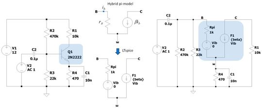
The term invariant equally applies to the bipolar and the PWM switch models, meaning that internal equations do not change, whatever the electrical configuration. For instance, the hybrid-π model could be used in a common-collector or common-base configuration, its internals won’t vary and you don’t have to tweak the model based on the electrical diagram you are dealing with. Same goes for a switching converter in which the PWM switch will take place. Whether the PWM switch model is plugged in a buck, a flyback or a SEPIC, the expressions linking the three terminals (a for active, p for passive and c for common) remain identical. It is truly one of the strengths of this approach compared to SSA. It means that if, later, you want to add a front-end filter or include more ohmic losses in the switching paths, the model does not change, just update the electrical diagram.
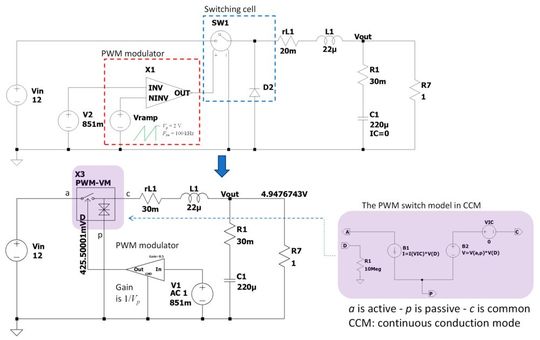
Figure 3 shows how this equivalent invariant large-signal model of the switching cell is inserted in place of the original circuit involving the switch and the diode. The switching cell is now described by a time-continuous network which can be simulated by SPICE in a .AC analysis. The solver will linearize the circuit around a dc operating point and delivers the ac response the designer wants to plot. In the original switching circuit, a naturally-sampled pulse-width modulator (PWM) generates the driving waveform to actuate the power switch on and off. The toggling event occurs when the artificial sawtooth intersects with the control dc voltage. With a value of 851 mV and a peak sawtooth voltage of 2 V, the corresponding duty ratio will be 0.851/2 = 425 mV or 42.5% considering a 1-V full scale for the D input of the PWM switch model. To model this block, a simple gain of 1/Vp will do and it is the 0.5 gain you see in the average model.
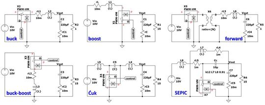
For studying most of the classical circuits, the implementation of the PWM switch is straightforward. That is what I have represented in Figure 4. Sometimes, you need to reveal the common connection of the switch and diode by transforming the circuit. It is the case for the SEPIC or the Ćuk converter for instance. Isolated topologies such as the flyback or the forward can also be easily modeled by adding a perfect transformer. Additional details about deriving and implementing the PWM switch will be found in reference [3].
We now have a look at how to implement this approach in three-phase power factor correction circuits (PFCs).
Three-phase PFC simulations
In this short article, we cannot review all the topologies suitable for building three-phase PFCs. We will concentrate the analysis on a 6-pack version, a popular structure which is naturally bi-directional. Figure 5 shows a possibility to control it with a dq0 algorithm. In a nutshell, this technique synthetizes the three rotating input current vectors into one single space vector via the Clarke transformation. This vector is then processed by the Park transformation to become two dc components, d (direct) and q (quadrature), respectively representing the active and reactive power (in a PFC application). A regulation loop adjusts these components to ensure a sinusoidal current absorption with a regulated output voltage. q is often set to zero (for a near-unity power factor) but not always as some applications require the circulation of reactive current.
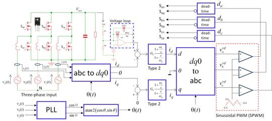
A second inverse-transform block builds the three new current setpoints from the dc-controlled d and q variables (id and iq in Figure 5) and drives the six transistors via dedicated modulators and drivers.
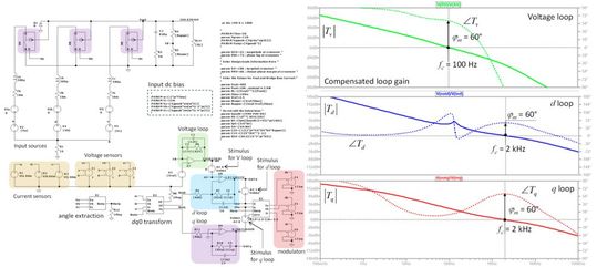
As with any closed-loop system, stability analysis must be carried over the three loops, with different compensation goals. For example, unlike with single-phase PFCs, the crossover frequency of the voltage regulation loop can be pushed up to 100 Hz as there is no low-frequency ripple on the output capacitor. For the d and q loops, crossover frequencies of a few kHz are usually well suited for a digital control system.
The control-to-output transfer function of these three loops can be obtained in different manners, including mathematical analysis and simulation with an averaged model as documented in Ref. [4]. In this paper, authors identify the PWM switch as a potential candidate to model a three-phase PFC but without presenting a simulation diagram. It is what I propose in Figure 6 with three PWM switch models in action. The input currents are sensed via three H sources, scaling the reading by a 80-mΩ ratio. These voltage images will feed the dq0 transform block which, together with the Θ angle extracted from the input voltages, delivers the instantaneous dc values for the d and q variables. Type 2 compensators then individually shape the ac responses of the three loops and confirm the good compensation strategy as shown in the right side of the figure.
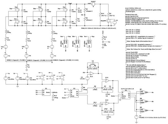
In parallel with the average model simulations, I have built a cycle-by-cycle switching circuit made of perfect switches for speeding the simulation up (Figure 7). Once all is working as expected, you can improve the schematic by modeling the drivers and inserting SiC MOSFET models (or IGBTs). Before upgrading a working circuit with imported models, I recommend you validate them via a double-pulse test as described in Ref. [5]. This test is important if you don’t want to waste time with long simulations finally leading to wrong results.
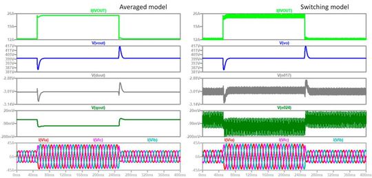
Now that our circuit has been stabilized, we can run a transient test and verify the corresponding waveforms. In this 400-V converter supplied from three 120-V ac sources (three-phase 208-V network), the output power is stepped from 5 to 10 kW with a few amperes per microsecond slope. The left side of Figure 8 depicts results delivered by the averaged models in a few seconds. The input signals are well sinusoidal and the drop of the output voltage remains below 20 V, with a clean recovery, without noticeable overshoot. The transient responses of the d and q loops are also extremely stable, confirming the adopted compensation strategy. The right side of the figure shows the same waveforms but, this time, obtained with the switching circuit. If we could superimpose the curves in LTspice, the averaged values would exactly match the switching waveforms. This confirms the excellent correspondence between the models and the cycle-by-cycle circuit. So not only you can trust the ac response, but you can also carry many different tests on the averaged circuit, being confident that it will faithfully reproduce what the switching circuit would do, but with at the expense of a longer simulation time.
Beside drastically reducing the simulation time, an average model lets you run many different tests like Monte Carlo or extreme value analysis (EVA) to test how component tolerances affect the stability or the total harmonic distortion (THD) as possible usage examples.
These PFC simulation examples, as well as many more, can be freely obtained by downloading my ZIP file through the link provided in Ref. [6].
Conclusion
This article has described how to use average models for simulating the complex architecture of a 6-pack three-phase power factor correction circuit. These models are useful for studying the small-signal response of the multiple loops found in this complicated converter. Once the dynamic response is obtained, the designer can select an adequate compensation strategy and immediately check the results on a transient response to a load step. The comparison between average modeling and a switching circuit confirms the validity of the approach.
References
- 1. S. Ćuk, Modelling Analysis, and Design of Switching Converters, Ph. D. dissertation Caltech, 1976
- 2. V. Vorpérian, Simplified Analysis of PWM Converters using Model of PWM Switch, parts I and II, IEEE Transactions on Aerospace and Electronic Systems, Vol. 26, NO. 3, 1990
- 3. C. Basso, Switch-Mode Power Supplies, Second Edition: SPICE Simulations and Practical Designs, McGraw-Hill, 2014
- 4. H. Mao, D. Boroyevich, F. Lee, Novel Reduced-Order Small-Signal Model of a Three-Phase PWM Rectifier and Its Application in Control Design and System Analysis, IEEE Transactions on Power Electronic, Vol. 13, NO. 3, 1998
- 5. C. Basso, Double-Pulse Test helps validating SiC SPICE models, PCIM News Platform, February 2025
- 6. C. Basso, Summer 2025 LTspice files collection, released in July 2025 from the author webpage
(ID:50946286)
:quality(80)/p7i.vogel.de/wcms/d6/9a/d69a90a148ae5222d27ac6b33c228a01/0131921521v2.jpeg "A compact three‑phase inverter platform based on the EPC33110 integrated GaN module delivers high switching frequency and power density for robotic joints and lightweight drone propulsion, combining monolithic half‑bridges, integrated drivers and simplified PCB layout. (Source: © Laura - stock.adobe.com)")
:quality(80)/p7i.vogel.de/wcms/f8/34/f834240d434a0c265a2ccafe614c8cd7/0134032109v4.jpeg "Hard- and soft-switching techniques shape voltage and current during device transitions, influencing switching losses, EMI and thermal performance in power converters. (Bild: © Mrthullab - stock.adobe.com)")