


:quality(80)/p7i.vogel.de/wcms/e9/5b/e95bc9c43c57018499c83a2c91ff9764/0132237640v2.jpeg "Yageo’s KH‑AT series automotive‑grade MOVs deliver robust surge absorption and stable electrical performance for demanding vehicle environments, protecting ECUs and power rails from transients. (Source: Yageo)")
:quality(80)/p7i.vogel.de/wcms/f4/61/f461d1f6bf3a6030877d90efced438f2/0132110372v2.jpeg "Taiyo Yuden’s new HVX and HTX hybrid conductive‑polymer capacitors offer AEC‑Q200 qualification, 80 V rating and high ripple capability at 135°C for noise suppression and power smoothing in automotive systems such as ADAS and power steering. (Source: Taiyo Yuden)")
:quality(80)/p7i.vogel.de/wcms/a4/b6/a4b6256bef45368325659f926c268ebe/0132104622v2.jpeg "Toshiba’s new 80 V N‑channel power MOSFET, built on the company’s latest process, improves conduction and switching efficiency for AI server power supplies and high‑frequency data‑center converters. (Source: Toshiba)")
:quality(80)/p7i.vogel.de/wcms/c0/c5/c0c5bdbaf6df6fdd0fecc97c419ea9b4/0132022612v2.jpeg "Magnachip’s 6th‑generation 600 V super‑junction MOSFETs deliver improved efficiency and thermal performance for AI server power supplies and EV fast‑charging systems. (Source: © AntonKhrupinArt - stock.adobe.com)")
:quality(80)/p7i.vogel.de/wcms/b0/6e/b06e82b69f8885bc8f32baadcb6e767d/0132481183v2.jpeg "CATL unveils six major innovations—from Shenxing superfast‑charging cells and Qilin condensed modules to Naxtra sodium‑ion technology—designed to boost range, lower charging times and scale battery production across EVs, energy storage and industrial applications. (Source: © Antonio - stock.adobe.com)")
:quality(80)/p7i.vogel.de/wcms/51/72/51726a890dc35d74f494908b29681028/0132478976v2.jpeg "Bosch intends to start U.S. based commercial manufacturing in 2026 – just three years after acquiring the Roseville site. (Source: Bosch)")
:quality(80)/p7i.vogel.de/wcms/cc/f5/ccf52ac525f49330b780868db8f9565c/0132364990v2.jpeg "Infineon and LS ELECTRIC sign a memorandum to co‑develop high‑efficiency DC power infrastructure for AI data centers and next‑generation grids, targeting power conversion, energy storage integration, solid‑state transformers and semiconductor circuit breakers. (Source: © Yuliia - stock.adobe.com)")
:quality(80)/p7i.vogel.de/wcms/c6/16/c616f00139ce1575d3292524579868ed/0132241890v2.jpeg "GlobalWafers and Micron announce a strategic collaboration—including proposed financing support and a long‑term wafer supply agreement—to strengthen U.S. wafer manufacturing capacity and shore up the semiconductor supply chain for AI and data‑center demand. (Source: © Fervix Neon - stock.adobe.com)")
:quality(80)/p7i.vogel.de/wcms/2d/39/2d39834eb64770ed52ca5dcef528fbcb/0132499809v2.jpeg "Sintered die attach, copper interconnects and ceramic‑brazed substrates replace solder and wire bonds to dramatically extend SiC/GaN module lifetime, reduce thermal resistance and cut commutation inductance for next‑gen high‑speed switching. (Source: © yasna - stock.adobe.com)")
:quality(80)/p7i.vogel.de/wcms/6b/1a/6b1a36faaaf922713b363d3f6cbce8dc/0132482196v2.jpeg "Agrivoltaics is also known as solar farms, agrophotovoltaics, agrisolar, and dual-use solar. (Source: © Anas - stock.adobe.com)")
:quality(80)/p7i.vogel.de/wcms/cc/60/cc6053a28d072fb3b965bd058547a0c2/0132501535v2.jpeg "The 200 mm SiC ramp and Chinese substrate price pressure are reshaping power‑semiconductor economics while GaN supply moves to new foundries and 300 mm lines — a bifurcated market with GaN density below 650 V and SiC dominance above 1.2 kV. (Source: © roei - stock.adobe.com)")
:quality(80)/p7i.vogel.de/wcms/56/df/56df94563ff47bb9d2009e419f7d4106/0132521528v2.jpeg "This article shares an overview of selecting gate drivers for silicon and wide-bandgap semiconductors. (Source: © starush - stock.adobe.com)")
:quality(80)/p7i.vogel.de/wcms/7b/76/7b76005554b556df2a7a3794bdf69d44/0132365246v2.jpeg "Hioki’s ST5680A DC Hipot Tester combines CE/UKCA/CSA compliance, an integrated capacitance‑based contact check and time‑series waveform recording (voltage, leakage current, insulation resistance) to standardize hipot and insulation testing across EV cell, module and pack production lines. (Source: Hioki)")
:quality(80)/p7i.vogel.de/wcms/af/7f/af7f7b0fb7f29219fc991b1130f65477/0132241333v2.jpeg "Comprehensive laboratory testing regimens—combining thermal cycling, high‑current stress, EMC, and accelerated lifetime tests—are essential to validate advanced power designs and ensure reliability in real‑world applications. (Source: PRBX)")
:quality(80)/p7i.vogel.de/wcms/16/3d/163df69363f8125315a9826e13ea4b05/0131927425v2.jpeg "Solution will maximize data center and AI factory profitability while delivering engineering-grade insights to design and operations for more efficient, sustainable, and resilient infrastructure. (Source: Cadence)")
:quality(80)/p7i.vogel.de/wcms/85/b7/85b7e90733a2bd8f21515d8f7137f2fc/0131917677v2.jpeg "Renesas acquires Pictorus to integrate its embedded application software platform with Renesas’ MCU and MPU portfolio, helping developers shorten time‑to‑market and simplify system integration. (Source: © lucadp - stock.adobe.com)")
SIC MODULES Beyond wire bonds: The advanced packaging revolution inside power modules
Related Vendors
:fill(fff,0)/p7i.vogel.de/companies/60/7e/607ec89d5d9b5/white-frame.jpg "white frame.jpg (www.rohm.com)")
:fill(fff,0)/p7i.vogel.de/companies/5f/71/5f71d5f92a5f6/2000px-rogers-corporation-logo-svg.png "2000px-Rogers_Corporation_Logo.svg.png (rogers germany)")
:fill(fff,0)/p7i.vogel.de/companies/66/8b/668becd1c07eb/dowa-logo-word--1-.jpeg "dowa-logo-word--1- (DOWA)")
Packaging materials account for roughly a third of a power module's cost, and in modern SiC modules, they increasingly set its lifetime too. A silver-sintered die attach survives around 22 times more power cycles than a soldered one in Infineon's published testing, a silicon nitride AMB substrate withstands 5,000 thermal shock cycles where standard alumina DBC fails at 55, and embedding the die in the substrate cuts commutation loop inductance from tens of nanohenries to roughly one.
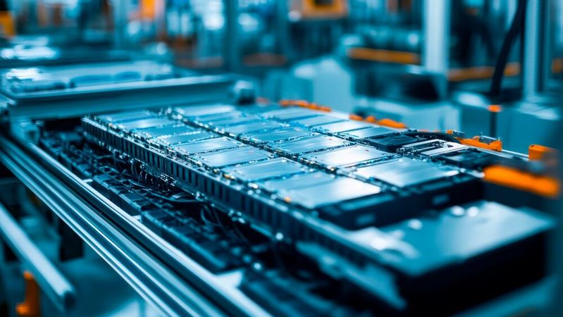
With SiC and GaN dies now switching at slew rates their packages were never designed for, the solder joints and aluminum wires that defined power modules for four decades are being replaced, layer by layer.
Die attach, from solder to sintering
A standard SAC solder joint melts at 217 to 220°C and conducts heat at under 65 W/mK, which leaves little margin in a module whose SiC die is rated for 175°C junction operation and could physically tolerate more. Under repeated power cycling, the joint's grain structure coarsens, voids form and link into cracks, and thermal resistance climbs until the die overheats. Sintered silver replaces the joint with a porous metal layer formed below 250°C that then behaves like bulk silver, melting at 961°C, conducting at 150 to 250 W/mK, and coming out roughly 70% thinner than a solder bond line, per Semikron Danfoss, which has run silver sintering in mass-produced modules since 2007.
Infineon's .XT interconnect technology, which pairs sintered die attach with copper wire bonds, logs around 225,000 power cycles at a 175°C maximum junction temperature and 2-second on-time, against around 10,000 for the standard soldered and aluminum-bonded stack, and keeps working at 200°C, where the older construction can't operate without severe derating. Heraeus Electronics claims up to 10 times the power cycling lifetime for its pressure-sintered silver pastes, and a more conservative four times module lifetime for a fully sintered module versus a fully soldered one. Sintered layers also cut peak die temperature by more than 10°C in the company's testing, and every 10-degree reduction roughly doubles die lifetime.
Silver's cost keeps the pressure on for an alternative, and copper sinter pastes are the leading candidate: copper runs around 100 times cheaper than silver as a raw material, but oxidizes readily and needs a protective atmosphere through drying, placement, and sintering, so the process ecosystem is still maturing. Equipment makers are moving first. ASMPT's SilverSAM PRO sinter press platform, shown at PCIM Europe 2026 in Nuremberg in June, ships with an oxidation-free process chamber designed explicitly for copper-compatible sintering on DBC and AMB panels.
:quality(80)/p7i.vogel.de/wcms/03/17/0317acd95b1c48654878e771db0c9308/0127124379v2.jpeg "0127124379v2 (Source: Kirill Klein)")
PART 1: FROM IDEA TO CONCEPT – GENERAL CONSIDERATIONS
Introduction to Holistic 7D Power Module Design
Interconnect, from wire bonds to clips and embedded die
A single 500-micron aluminum bond wire fuses at about 35 A, so high-current modules parallel dozens of them, and every one is a fatigue site. Aluminum expands at around 23 ppm per degree Celsius, against silicon's 3, and each thermal cycle flexes the bond heel until it cracks or the foot lifts off the die. Aluminum ribbon raised the ceiling, with a 2,000 by 300-micron ribbon carrying around 105 A in place of three heavy wires, but the geometry and the fatigue mechanism stay the same.
Copper clips remove the wire entirely, replacing it with a stamped plate soldered or sintered across the die's top surface. Danfoss's Bond Buffer process shows what the copper transition is worth even in wire form: a sintered copper buffer on the die enables copper wires with a bonded cross-section more than 20 times larger than conventional wiring, a 9% cut in thermal resistance, and a 100 mV lower forward voltage drop at 200 A. The approach has automotive precedent at scale, since the Tesla Model 3's inverter used 24 molded STMicroelectronics SiC modules with copper ribbon connections rather than aluminum wire as far back as 2018.
Embedded die goes further and eliminates the loop itself, and the math behind it is unforgiving. At 10 A/ns, every 10 nH of loop inductance adds 100V of overshoot on top of the bus voltage. A discrete TO-247 contributes 5 to 7 nH of package inductance before the PCB loop is counted, while Infineon's embedded 1,200V CoolSiC S-cell measures around 2 nH, and its p2PACK program with Schweizer Electronic has run 1,200V, 11 mΩ embedded SiC in a 50 kW evaluation at 900V input.
Fraunhofer IZM and Mitsubishi Heavy Industries published a 500 kW-per-liter SiC inverter in June 2026, built on AMB chip embedding, with six paralleled 1,200V dies per switch, a primary commutation loop of about 1 nH, 65 V/ns slew rates, and better than 99% efficiency at 500 ARMS. At PCIM Europe 2026, ASE subsidiary USI showed SiC die embedded in multilayer ABF substrates targeting 400V and 800V EV inverters and AI data center power, a sign of how much OSAT interest the format is drawing.
:quality(80)/p7i.vogel.de/wcms/86/f4/86f4bafd5bb61f9bcca9d0d483d08a83/0131829744v2.jpeg "New 1200 V trench‑gate SiC MOSFET samples from Toshiba enable higher efficiency and improved thermal performance for compact, high‑power converters. (symbolic image) (Source: © han - stock.adobe.com)")
POWER SEMICONDUTORS
Toshiba develops SiC power module technology for high-frequency inverters
Substrates and double-sided cooling
The ceramic under the die faces the same escalation. Standard 96% alumina DBC conducts at 24 W/mK and survives around 55 thermal shock cycles between -55 and 150°C before the copper delaminates; aluminum nitride DBC conducts far better at 180 W/mK but is brittle, with the lowest fracture toughness of the common ceramics, and fails the same test at around 35 cycles.
Silicon nitride brazed under an active metal braze (AMB) process conducts at 90 W/mK, carries roughly double the flexural strength of either alternative, and passes 5,000 cycles of the same test. Fracture toughness, not bending strength, turns out to be the property that predicts substrate life, and Si3N4's 6.5 to 7 MPa·m0.5 is roughly double AlN's. Thicker copper for higher current density is a side benefit of the braze, and it's why Si3N4 AMB has become the default under high-power SiC.
Substrate suppliers are scaling in response, with Rogers expanding curamik AMB capacity into China after enlarging its German plant, and research programs such as the PVA TePla and Fraunhofer IISB joint lab working on aluminum nitride crystal growth for the next substrate generation.
Yole values power module packaging raw materials at $4.1 billion by 2028, around 28% of total module value, growing at 11% annually through 2030 per its latest packaging report. Wolfspeed's 2025 YM six-pack, with sintered die attach and copper clip interconnects, claims three times the power cycling capability of its predecessor, and Infineon's CoolSiC G2 EasyPACK modules running .XT interconnect at 175°C with 200-degree overload capability shows where volume production is.
The SiC or GaN die in a well-designed 2026 module is no longer the component that wears out first, and keeping it that way is now the packaging engineer's problem.
(ID:50909741)
:quality(80)/p7i.vogel.de/wcms/b7/ae/b7aef5b0ab72c24edd51f8318d4029c4/0127137768v2.jpeg "From raw materials to system demonstrators: FastLane strengthens Europe’s technological sovereignty. (Source: © Adobe Stocks, modified by Heraeus Electronics
)")
:quality(80)/p7i.vogel.de/wcms/72/fa/72fa65ac052da71dd3fcef19cd75f16b/0126978972v2.jpeg "Integrated power modules simplify motor control by combining essential components into a compact package, enhancing design efficiency and market speed for appliances and HVAC systems. (Source: Dall-E)")