MICROFABRICATION Tiny titans: Unveiling the power of 2nm and 1nm chips
Related Vendors
While the three-nanometer chip is going to witness a shortage, people on the internet are talking about the chips produced through two-nanometer and one-nanometer processes. Chip-making giants like TSMC, Intel, Samsung Semiconductors, and many more have publicly announced plans to move to two-nanometer and one-nanometer nodes in the upcoming six years. The article explains the latest news about 2-nm and 1-nm chips with their actual meaning and features.

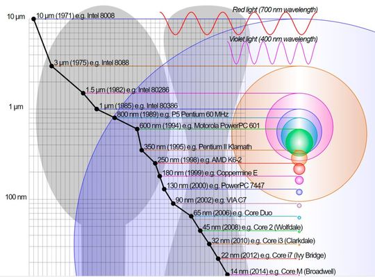
The current transistor technology uses 7-nm, 5-nm, and 3-nm technology nodes. Looking at the transistor count history, the three-micrometer node was used in 1987. The initiation of the nanometer node happened 20 years ago through the introduction of the 90-nm process.

As of 2022, the 3-nm technology node was the smallest to be commercialized. Apple’s iPhone 15 Pro and iPhone 15 Pro Max uses TSMC 3-nm chip. According to the latest buzz, the 3-nm chips are reportedly facing shortage due to high demand as all are nearly booked for the next two years.
In 2021, IBM introduced the smallest 2-nm node chip. However, such technology is in the testing phase- yet to be commercialized. All these 3-nm and 2-nm chips improve efficiency and eventually function as AI semiconductors.
Release of two-nanometer and one-nanometer chips
The chip race to achieve the smallest but efficient product has been continuing for years. The current smallest chip battle is to produce chips based on 2-nm and eventually 1-nm processes. TSMC (Taiwan Semiconductor Manufacturing Company), Intel, and Samsung have confirmed their plans to produce 2nm and 1nm chips in the coming 2-3 years. TSMC plans to commercialize 1.6-nm chips by 2026.
Similarly, Samsung is all set to launch 2-nm chips by the end of 2025 and 1.4-nm chips in 2027. Intel plans to launch 2-nm and 1.8-nm chips by 2025, and 1-nm chips by late 2027. The US Chips Act benefits these chip-makers through multi-billion dollar funds for producing smaller and better chips in their country. All chip-making giants plan to test and launch the 2nm process into 2025 and initiate mass production by 2027.
:quality(80):fill(efefef,0)/p7i.vogel.de/wcms/5f/fe/5ffedb2e0ffa6/listing.jpg)
What are two-nanometer and one-nanometer chips?
In semiconductor manufacturing, the terms “process”, “process node” and “technology node” are used interchangeably for 2nm, 1nm, and other nm chips. This is because all these terms represent the manufacturing process involved in chip size shrinking with a high transistor count.
In simple words, any nanometer process/technology node is a manufacturing process rather than a unit of length. The chips produced through these nanometer processes are commonly called nanometer chips. For example, the chips produced through the 2-nm process are called 2-nm chips. Similarly, chips produced through the 1-nm process are called 1-nm chips.
All the technology nodes: seven-nanometer, five-nanometer, three-nanometer, two-nanometer, and one-nanometer are marketing terms to produce smaller and more efficient ICs with high transistor count. The 5-nm process produces smaller ICs with a high transistor count compared to the 7-nm process. Similarly, a 2-nm process would produce efficient and smaller ICs with a higher transistor count than the current 3-nm process.
Is “nanometer” in the X-nm node a misnomer?
It was a common misconception that the nanometer represents the length of the gate of the transistor. The usage of “nanometers” in the 1nm process is correct because the gate length is actually in nanometers but not exactly one nanometer. The distance between the centers of two adjacent transistor gates in an IC is called gate pitch. Similarly, the distance between the centers of two adjacent metal lines in an IC metal layer is called metal pitch.
The term nanometer in the X-nm processes may point out values of gate pitch and metal pitch expressed in nanometers. The gate pitch in the 5-nm process was 51 nm and 48 nm in the 3-nm process. The metal pitch in the 5-nm process was 30 nm and 24 nm in the 3-nm process. None of the lengths were 3nm or 5nm. However, the size of the transistor is significantly reduced for lesser technology nodes.
Why are gate and metal pitches important?
A transistor has three terminals: gate, source, and drain. The gate is a controlling terminal that controls the current flow between the other two terminals. The voltage at the gate terminal controls transistor switching action: the transition between on and off states.
The gate is the insulated terminal of the transistor. All transistors in chips are connected through gate terminals. The smaller the gate is, the smaller the transistor gets. The term technology node is often mistaken to be gate length.
Interconnects are critical to allow current flow in the chip for improved processing and storing capabilities. Metal pitches affect the compactness through routing and wiring density. Hence, smaller gates and metal pitches are indicators of high efficiency.
:quality(80)/p7i.vogel.de/wcms/90/1b/901be2f3de5787e00dcd5d7fafa59333/0119258051v2.jpeg)
CHIP SHORTAGE NEWS
The global semiconductor crisis: A review of Q2 2024
Features of 2-nm and 1-nm chips
Die shrink
These nanometer processes are compliant with Moore’s law. Despite multiple arguments, Moore’s law still holds true for transistor feature sizes and all the listed technology nodes. Small-sized transistors enable large-scale integration in a chip. As a result, smaller dies (chips on a wafer) have enhanced processing capabilities, performance, speed, and storage capacity.
| Technology Node | Gate Pitch | Metal Pitch |
| 2-nm | 45 nm | 20 nm |
| 1-nm | 42 nm | 16 nm |


:quality(80)/p7i.vogel.de/wcms/f5/d2/f5d2bce7c01775fe62d4c6ecebc8c5ba/0129188745v2.jpeg)
:quality(80)/p7i.vogel.de/wcms/cb/38/cb38bf951c0af8a8de423fedce2489d8/0129352475v2.jpeg)
:quality(80)/p7i.vogel.de/wcms/b8/13/b8139abf82c98aa04248a4a119d28c13/0129194616v2.jpeg)
:quality(80)/p7i.vogel.de/wcms/62/80/6280da00d591873bf8f0b2a70e5986e0/0129064771v4.jpeg)
:quality(80)/p7i.vogel.de/wcms/60/40/6040b2e00aef20b4f9d92e8ac9f79c32/0129349725v2.jpeg)
:quality(80)/p7i.vogel.de/wcms/b3/13/b313941dbf7adc57c6d144966106d82b/0129219607v2.jpeg)
:quality(80)/p7i.vogel.de/wcms/56/a4/56a4d9b6ee131a7a00b8b89dabf108f9/0128979281v2.jpeg)
:quality(80)/p7i.vogel.de/wcms/67/62/676279913d77e1db48eb5cbe9be4c767/0128937895v2.jpeg)
:quality(80)/p7i.vogel.de/wcms/f0/d8/f0d82f06ed1b7abb3245dfc4c317cb55/0127949994v2.jpeg)
:quality(80)/p7i.vogel.de/wcms/6e/e5/6ee5ad1dc45fd69a5a5718147605850a/0129347492v2.jpeg)
:quality(80)/p7i.vogel.de/wcms/7d/40/7d406bd959b3a9127c33a66157f9030a/0128339184v4.jpeg)
:quality(80)/p7i.vogel.de/wcms/65/22/65223bc58811ced76adbfa7b5615d532/0129061536v2.jpeg)
:quality(80)/p7i.vogel.de/wcms/23/ee/23ee4a97790d6009dbfd7d9577ffa723/0129220424v2.jpeg)
:quality(80)/p7i.vogel.de/wcms/3c/d1/3cd1cacbceb792ba63727199c61ca434/0127801860v2.jpeg)
:quality(80)/p7i.vogel.de/wcms/5a/a0/5aa0436498af618297961fd54ab36cdf/0126290792v2.jpeg)
:quality(80)/p7i.vogel.de/wcms/cb/30/cb30ebdca7fcaea281749cb396654eb3/0124716339v2.jpeg)
:fill(fff,0)/p7i.vogel.de/companies/60/7e/607ec89d5d9b5/white-frame.jpg)
:fill(fff,0)/p7i.vogel.de/companies/62/95/6295c25c8dc1a/schunk-sonosystems-300dpi.png)
:fill(fff,0)/p7i.vogel.de/companies/66/43/66433a241a49d/aurubis-logo-wc-p-rgb-300px.jpeg)
:quality(80)/p7i.vogel.de/wcms/37/f0/37f0579b316150e010442b4d4f820171/0122207252v2.jpeg)
:quality(80)/p7i.vogel.de/wcms/c2/f1/c2f1acbcc59fdf2cf17b6fe0a7bf7a1d/0125393004v2.jpeg)