BASIC KNOWLEDGE – MOSFET MOSFET – The most popular transistor explained
Related Vendors
Out of 13 sextillion manufactured transistors, MOSFET wins the game to become the most popular transistor. In most cases, the word “semiconductor” comes down to MOSFET only. The article explains everything about MOSFETs including their construction, working, and applications.
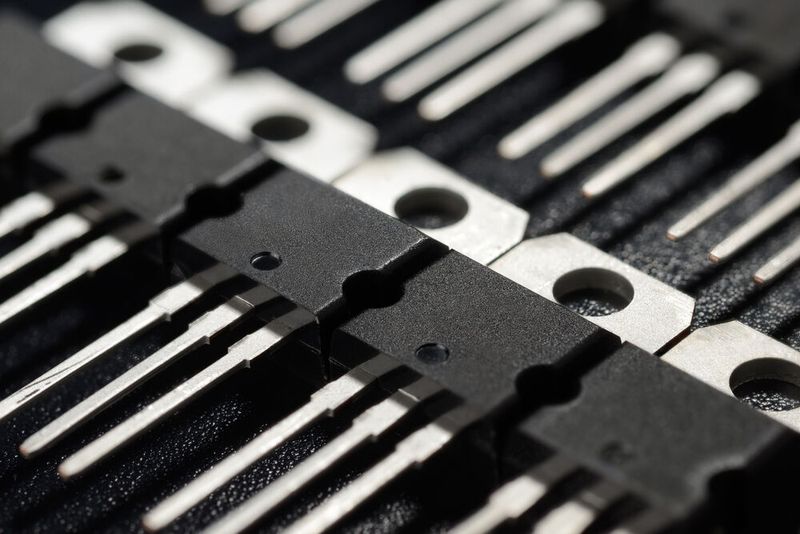
November 1959 marks 65 years of MOSFET invention. Two Bell lab researchers Mohamed Atalla and Dawson Kahng invented MOSFET. The invention was theorized and planned for years. Nothing was successful. As soon as VLSI gained momentum in the late 70s, MOSFETs became the most commonly used transistor worldwide.
What is a MOSFET?
MOSFET is used as a discrete component in switching and amplification circuits. The most common use of MOSFETs is in the form of integrated circuits (chips). They are integrated into billions and trillions on a computer chip.
MOSFET definition
Metal Oxide Semiconductor Field Effect Transistor “MOSFET” is a three-terminal voltage-controlled device used in electronic applications. A MOSFET transistor is a type of insulated gate field effect transistor (IG-FET) that uses an isolated gate terminal to control the resistance of its conductive channel.
Why using a MOSFET?
High input impedance
The input impedance of MOSFETs is higher compared to JFET. Impedance typically correlates to resistance. Having zero input impedance means no resistance to the input current or voltage signal. The signal is 100 % accepted for further operation. In addition, MOSFETs have a lower on-state resistance.
Voltage-controlled device
MOSFET transistor is a voltage-controlled device. The gate-to-source voltage VGS enables controlling the current flow in the circuit. MOSFETs are thermally stable and are easier to operate– compared to current-controlled devices. As a result, MOSFETs consume less power in practical applications.
Miniaturization
MOSFET transistor fabrication is common worldwide. They are fabricated with millions and billions on a single chip. Even as a stand-alone device, the size of a MOSFET is much smaller compared to other transistors.
MOSFET applications
Power Electronics
MOSFETs are used in power electronic applications that require high-voltage processing. They are used in power supplies, inverters, and DC-DC converters.
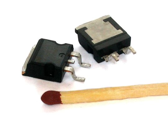
MOSFET as a switch
A MOSFET as a switch exhibits a high switching frequency. They are used as switches in various applications such as power electronics, LED lighting, automotive, control, medical devices, consumer devices, renewables, and many more.
MOSFET as an amplifier
MOSFETs function as amplifiers in various audio, power, and RF applications. In RF amplifiers, MOSFETs amplify radio frequency and microwave signals. Similarly, they are used in audio amplifiers and speakers to improve the sound quality.
Integrated circuits
Millions and trillions of MOSFETs are embedded in semiconductor chips (Integrated Circuits) for logic operations and memory storage. Due to low power consumption, MOSFETs are used in microprocessors to perform logic operations.
:quality(80):fill(efefef,0)/p7i.vogel.de/wcms/5f/fe/5ffedb2e0ffa6/listing.jpg)
Logic gates
Logic gates are building blocks of digital circuits. MOSFETs are used in AND, OR, NOT, NAND, NOR, EXOR, and EXNOR gates for binary signal processing. NOT gate is the most basic type of CMOS inverter.
Automotive applications
MOSFETs are used in electric powertrains, battery management, charging infrastructure, motor drivers, and motor control mechanisms in commercial vehicles and EVs.
The structure of a MOSFET explained
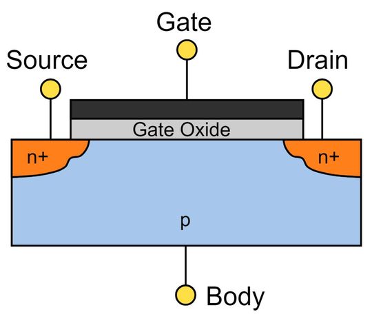
The basic MOSFET structure consists of a substrate. The entire Metal Oxide Semiconductor Field Effect Transistor structure is fabricated over the substrate. The structure consists of two heavily doped regions. The three terminals are gate (G), drain (D), and source (S). Drain and source terminals are extracted from metallic contacts placed on heavily doped regions.
The entire surface of the substrate is coated with an insulating layer of silicon dioxide. A metal plate is placed on the insulating layer to take out the gate terminal. There is no connection between the gate terminal and the substrate.
In some discrete MOSFET transistor versions, there is a fourth terminal called the body (SS). This terminal represents the substrate of the MOSFET transistor. In most cases, MOSFETs do not have an additional body terminal as it is internally connected to the source. However, the body terminal is not involved in controlling the current flow.
The gate is a “controlling” terminal that “controls” the conductance of the channel. The drain and source are “controlled” terminals. In general, the drain is the positive terminal and the source is the negative terminal of the MOSFET.
Why is MOSFET called “MOSFET”?
The silicon dioxide layer that isolates the gate terminal and metal contact surface is dielectric in nature. The term “dielectric” showcases the repulsion of the applied electric field.
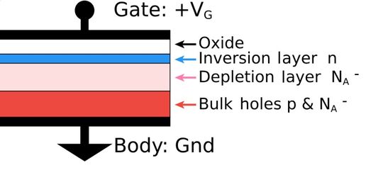
The silicon dioxide insulating layer is responsible for MOSFET’s high input impedance. It is also the reason for naming the device as a metal oxide semiconductor field effect transistor.
How does a MOSFET work?
A MOSFET transistor works by controlling the value of gate-to-source voltage. This voltage is responsible for controlling MOSFET’s drain current. The drain current is the output current of the MOSFET. Section 7 details the operation of MOSFET below.
The four variants of the MOSFET symbol described
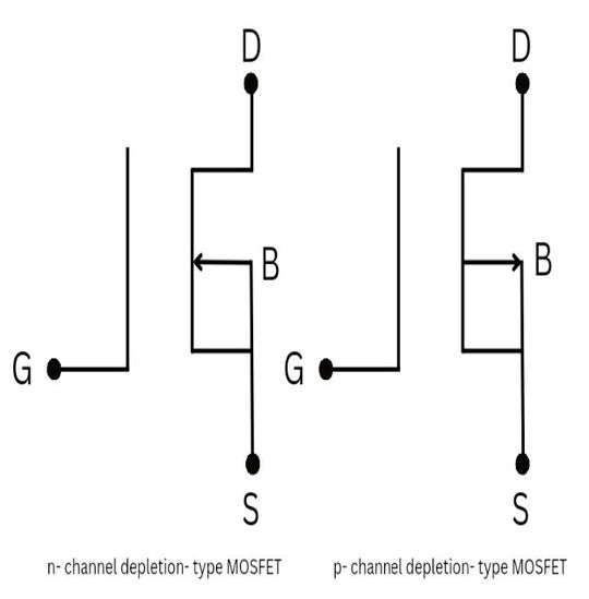
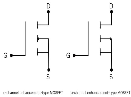
Each Metal Oxide Semiconductor Field Effect Transistor type is represented by a different symbol. All MOSFET symbols represent the real-world construction with the isolation of the gate terminal. The symbols of enhancement mode MOSFETs are nearly the same. Similarly, symbols of depletion mode MOSFETs are nearly the same.
The direction of the arrow in both n-channel and p-channel MOSFETs is different. The arrow represents the current flow direction. It is different in both p-type and n-type configurations in all transistor types.
Depletion mode MOSFET symbol
In depletion mode MOSFET symbols, the three terminals: drain, body, and source are connected. This connection line showcases the presence of a pre-manufactured conducting channel. The gate terminal is shown to be isolated from the channel. The body terminal is shorted to the source terminal.
Enhancement mode MOSFET symbol
In enhancement mode MOSFET symbols, the three terminals stand separately. This showcases that no channel was manufactured in the device. The gate remains isolated. The body terminal is shorted to the source in the enhancement mode MOSFET.
The types of MOSFET explained
The main difference between the depletion mode and enhancement mode of the Metal Oxide Semiconductor Field Effect Transistor is the presence of a conducting channel. In depletion mode MOSFETs, a conducting channel is constructed with the help of doping. There is no conducting channel manufactured in enhancement mode MOSFETs. The presence of conducting mode enables quick turn-on operation for depletion mode MOSFETs compared to enhancement mode MOSFETs.
N-channel is a negatively charged channel with electrons as the majority charge carriers. P-channel is a positively charged channel with holes as the majority of charge carriers.
N-channel depletion mode MOSFET
An n-type depletion mode Metal Oxide Semiconductor Field Effect Transistor consists of a p-type substrate, which is made from silicon. The substrate functions as the base on which the entire device is fabricated. Two heavily doped N-type regions are diffused on the substrate. There are two metal contacts that enable connecting the drain and source terminals to these n-doped regions. In addition, these two n-doped regions are connected through a channel made from an n-type material.
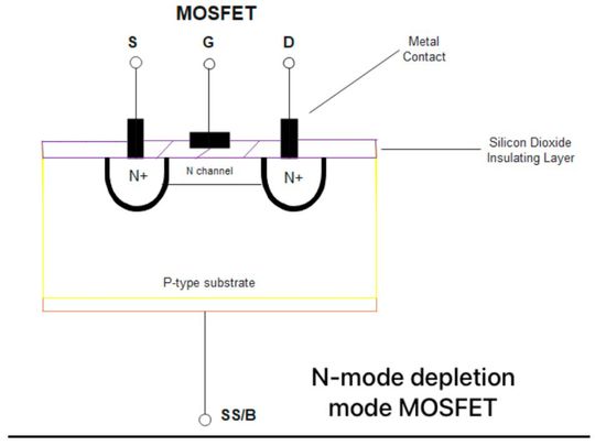
The drain terminal is connected to the positive terminal of the battery through a load resistor. The source is connected to the negative terminal of the battery and the ground. Voltage VDD appears across the battery. The voltage between the drain and the source terminal is called VDS or drain-to-source voltage. VDS is the output voltage of the MOSFET transistor.
The body terminal (SS) is connected to the source internally. The gate terminal is connected to a voltage source lesser than the voltage at the source terminal. In some cases, the gate terminal might be connected to a microcontroller, voltage divider network, or directly ground. The voltage between the gate and source terminals is called VGS. VGS is the input voltage of the MOSFET.
:quality(80)/p7i.vogel.de/wcms/f9/29/f92903189bb36304a6bbc7ca5ba8e3fc/0117522391.jpeg)
POWER ELECTRONICS
Inverter vs converter: What's the difference?
VDS = 0 V, VGS = 0 V
The gate-to-source voltage is set to zero by connecting the gate and source terminals with the ground. VDS is also zero. The channel is already present but no current flows through the device.
Ohmic Region: VDS > 0 V, VGS = 0 V
When a positive voltage VDS is applied to drain-to-source terminals, the electric field is established from drain to source. Free electrons in the n-channel start to incur a positive attraction force that pushes them to move toward the positive terminal of the battery.
Simply put, electrons start moving from source to drain. The conventional current flows from the drain to the source. The magnitude of current at VGS = 0 is called IDSS. The magnitude of the IDSS is very small in the order of milliamperes. A similar process is also seen in a JFET transistor.
VDS > 0 V, VGS = -1 V (Negative Voltage)
As negative voltage is present near the drain terminal, the resulting electric field is also higher near the same region. The gate-to-source voltage is set to a negative value, negative charge starts to accumulate over the gate terminal. A strong repulsive force is generated across the device. The electrons in the n-channel are forced to move towards the p-type substrate.
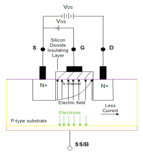
On the other hand, an attractive force attracts minority charge carrier holes from the p-type substrate towards the n-channel. Electron-hole recombination takes place at the surface. Accumulation of positive charge carriers near the gate terminal reduces the width of the n-channel. As the resistance increases, the current flow decreases.
The high magnitude of the negative input VGS voltage facilitates high recombination. The channel becomes narrower. The process of electron-hole recombination reduces the number of free electrons across the device. At about VGS = -6 V, pinch-off occurs. The channel depletes and the drain current almost reaches zero. The MOSFET transistor functions like an open switch— turns off. In simple terms, negative input VGS voltage reduces drain current flow.
VDS > 0 V, VGS > 0 V (Positive Voltage)
The connection makes drain and gate terminals positive with respect to the source terminal. When the gate-to-source voltage is set to a positive value, a positive charge accumulates over the gate terminal. Free electrons present in the MOSFET are attracted towards the gate terminal. The width of the channel increases.
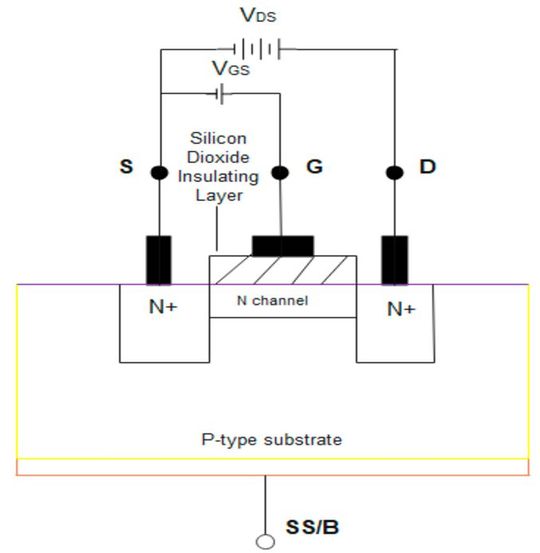
The dielectric nature of silicon dioxide prevents electrons from combining with the positive charge. More and more electrons tend to flow across the device. The collision of accelerating ions gives rise to new charge carriers, contributing to the overall drain current flow. Increasing input VGS voltage rapidly increases drain current flow.
The drain current increases beyond the saturation current IDSS. The drain current must increase within its rating to prevent the device from being damaged. As compared to JFETs, N-channel depletion-mode MOSFETs can operate for positive and negative values of VGS voltage.
P-channel depletion mode MOSFET
The construction of p-channel depletion mode MOSFETs is the opposite of n-channel depletion mode MOSFETs. A p-channel depletion mode MOSFET transistor consists of an n-type substrate on which the entire device is fabricated.
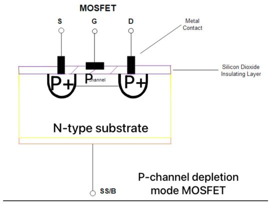
The substrate functions as the base on which two heavily doped p-type regions are diffused. The gate, drain, and source terminals are present likewise. Instead of an n-channel, a p-type channel connects these two p-type doped regions.
VDS > 0 V, VGS > 0 V
The p-channel consists of the majority of charge carrier holes. It is a positively charged channel. When the gate is given positive voltage, negative charges accumulate near the gate plate. Here, electrons are minority charge carriers that start to repel holes.
The holes in the p-channel are forced to move towards the n-type substrate. Excess of electrons degrades the positive character of the channel. As a result, the channel width reduces further. The high magnitude of positive VGS voltage stops the current flow. MOSFET functions like an open switch.
VDS > 0 V, VGS < 0 V
Similarly, a negative voltage at the gate accumulates loads of negative charge. Excess holes present in the p-channel get attracted towards the gate. As a result, channel width increases, and more drain current flows through the device.
N-channel enhancement mode MOSFET
The construction of an n-type enhancement mode MOSFET is slightly similar to a depletion mode n-type MOSFET. It also consists of a p-type substrate with diffusion of heavily doped n-type regions. The placement of the drain, source, and gate terminals are also the same. Unlike depletion mode n-type MOSFET, there is no n-type channel constructed in enhancement mode n-type MOSFET. The silicon dioxide is directly separated from the p-type substrate, without the n-channel.
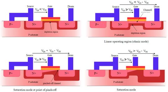
The drain terminal is connected to the positive terminal of the battery through a load resistor. The source is connected to the negative terminal of the battery and the ground. The gate terminal is connected to a voltage source lesser than the voltage at the source terminal. Similarly, voltages VGS and VDS play a key role in the operation of enhancement-type MOSFETs.
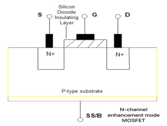
Cut-off region: VDS > 0 V, VGS = 0 V
At VGS = 0 V with some amount of voltage applied between the drain to source terminals, no channel formation takes place between the drain and source terminals. Two n-doped regions form two PN junctions with the P-type substrate material. The application of positive VDS reverse biases them. No current flows through the device. MOSFET operates in the cut-off region. This process was different in depletion-type MOSFETs.
Ohmic region: VDS > 0 V, VGS > 0 V
Drain and gate terminals are connected to the positive terminal of the battery while the source is connected to the negative. The positive potential at the gate terminal repels holes present in the P-substrate near the insulating layer of silicon dioxide.
The repulsive force pushes holes into the p-type substrate, slightly below the gate plate. Similarly, the gate terminal attracts electrons present in the p-type substrate. The insulating layer of silicon dioxide prevents them from escaping the region.
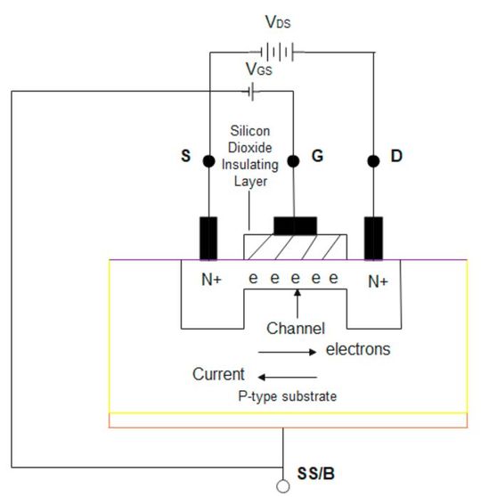
An electric field is established in the direction of the body. As VGS is increased further, excessive electrons accumulate near the gate plate. The region of the p-type substrate near the gate plate becomes “less p-type” and starts to exhibit “n-type character”. As a result, an n-type channel formation takes place in the device.
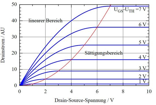
The minimum value of VGS at which the MOSFET transistor enters into the conduction mode is called threshold voltage or VTH. When VGS crosses VTH, the drain current starts to flow in the device. The process when VGS increases beyond VTH to form the channel is called inversion. The electrons flow from source to drain while the conventional current flows from drain to source.
VDS increased, VGS constant
If VGS is held constant and VDS is increased, the gate terminal becomes less and less positive. No electrons start to accumulate near the gate plate. The width of the channel reduces. The drain current reaches a saturation level instead. As positive VGS voltage increases or “enhances” the level of free charge carriers, the mode of operation is called enhancement mode.
P-channel enhancement mode MOSFET
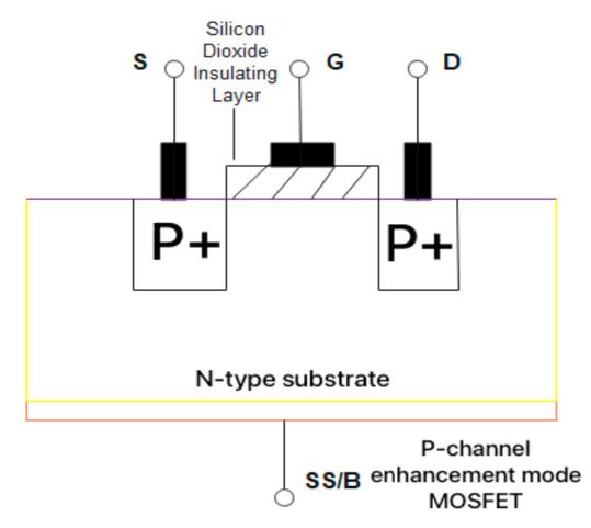
The construction of p-channel enhancement mode MOSFETs is the opposite of n-channel enhancement mode MOSFETs. A p-channel enhancement mode MOSFET transistor consists of an n-type substrate made from a silicon base. Similarly, two doped p-type regions are there in the device structure.
:quality(80)/p7i.vogel.de/wcms/f5/e5/f5e5d9e1e9f0511b1cb1403ba940bccc/87420887.jpeg)
BASIC KNOWLEDGE - MOSFET VS. BJT
What’s the difference between MOSFET and BJT?
All the gate, drain, and source terminals remain the same. However, the conducting channel is absent from the construction. There is no p-type channel that connects two p-type doped regions. Depending upon the polarity of gate-to-source voltage, a p-channel can be created.
VDS = 0 V, VGS = 0 V
A p-channel enhancement mode MOSFET does not operate without the application of gate voltage. No current flows through the circuit.
VDS > 0 V, VGS < 0 V
A negative gate voltage accumulates a significant amount of negative charge at the gate plate. Holes, being majorly present in the p-regions, are attracted towards the gate plate. Excess holes enable the creation of a conductive p-channel. Higher negative gate voltage increases the width of the channel. The drain current increases further as MOSFET conducts.
VDS > 0 V, VGS > 0 V
A positive gate voltage accumulates a significant amount of positive charge at the gate plate. Holes, being majorly present in the p-regions, are repelled towards the substrate. Excess minority charge carriers—electrons, gather near the gate plate to prevent the formation of the p-type channel. The drain current becomes negligible. MOSFET turns off.
MOSFET characteristics
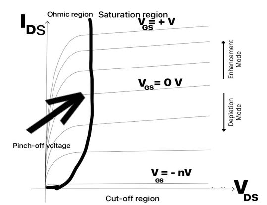
The drain characteristics of a Metal Oxide Semiconductor Field Effect Transistor is a graph of drain current ID on the X-axis vs drain-to-source voltage VDS on the Y-axis.
Depletion mode MOSFET
Depletion-type MOSFET transistors operate when gate-to-source voltage VGS is negative and positive both. Depletion mode MOSFETs operate in depletion and enhancement modes. Depletion mode depletes the channel while enhancement mode enhances the channel.
Depletion mode: When VGS is lower than 0 V, MOSFET operates in depletion mode. The pre-manufactured channel is depleted.
Enhancement mode: When VGS > 0 V, MOSFET operates in enhancement mode. The increasing positive gate voltage attracts more charge carriers to increase channel width. The MOSFET operation enhances the channel - increasing the drain current.
Enhancement mode MOSFET
Enhancement-type MOSFET operates only when the gate-to-source voltage VGS is greater than the threshold voltage. When VGS is lower than the threshold voltage, MOSFET remains off.
FETs Vs BJTs
Along with JFET, MOSFET is a type of FET. The table compares FETs and BJTs on a broader level.
| Feature | BJT | MOSFET |
| Name | Bipolar Junction Transistor | Metal Oxide Semiconductor Field Effect Transistor |
| Terminals | Base, emitter, and collector | Gate, drain, and source |
| Isolation | No isolated terminal | Gate isolated |
| Transistor-type | Bipolar | Unipolar |
| Device-type | Current controlled | Voltage controlled |
| Nature of current | Bipolar | Unipolar |
| Current conduction | Majority and minority charge carriers | Majority charge carriers |
| Types | P-type N-type | n-channel depletion mode p-channel depletion mode n-channel enhancement mode p-channel enhancement mode |
| Configuration | Common base Common emitter Common collector | Common gate Common source Common drain |
| Input impedance | Low | Very high |
| Temperature coefficient | Negative | Positive |
| Thermal stability | Less as BJTs are current controlled devices | More as FETs, including MOSFETs, are voltage-controlled devices |
| Thermal noise | More | Less |
| Switching speed | High | Low |
| Gain | High current gain Low voltage gain | Low current gain High voltage gain |
| Gain bandwidth product | High | Low |
| Size | Big | Small MOSFETs are about 5% of BJT size |
| Fabrication process | Complex | Easy and more common |
Conclusion
Historically, the small size of MOSFETs enabled faster scaling in commercial applications. Compared to BJTs, MOSFETs offer various advantages in dozens of electronic applications. They are chosen because of their low input impedance, switching speed, size, and thermal stability. All of this has eventually led to Metal Oxide Semiconductor Field Effect Transistor becoming the most common transistor worldwide.
Power Electronics in the Energy Transition

The parameters for energy transition and climate protection solutions span education, research, industry, and society. In the new episode of "Sound On. Power On.", Frank Osterwald of the Society for Energy and Climate Protection Schleswig‐Holstein talks about the holistic guidance his organization can provide.
Listen now!
(ID:50249183)


:quality(80)/p7i.vogel.de/wcms/2f/f3/2ff3221bf7665de2d0acf83760bfd1fa/0130031523v2.jpeg)
:quality(80)/p7i.vogel.de/wcms/c3/16/c316e955a97f5d72d9678297b237b9e5/0129932858v2.jpeg)
:quality(80)/p7i.vogel.de/wcms/ef/0a/ef0adb0acf793fe147cc27c21f6a7a67/0129954238v2.jpeg)
:quality(80)/p7i.vogel.de/wcms/53/f9/53f9301dfc9292d02960f7996c79cc6e/0129927601v2.jpeg)
:quality(80)/p7i.vogel.de/wcms/6e/cd/6ecd41d095d5111cf4ed37b714844487/0129930878v2.jpeg)
:quality(80)/p7i.vogel.de/wcms/02/c0/02c0e9722f70b1134dbf96fb59a9c73d/0129655179v2.jpeg)
:quality(80)/p7i.vogel.de/wcms/cc/67/cc670ea2029cd2af5c641af70e1bf734/0129816392v4.jpeg)
:quality(80)/p7i.vogel.de/wcms/ea/e6/eae6aee30071e67a5627027974437134/0129544613v2.jpeg)
:quality(80)/p7i.vogel.de/wcms/b1/5e/b15ee02b0ba02db70cf61e37d66ad1d3/0129349127v2.jpeg)
:quality(80)/p7i.vogel.de/wcms/26/d5/26d591cc340077026eac56a0e7564faf/0129949603v2.jpeg)
:quality(80)/p7i.vogel.de/wcms/4d/e0/4de02f76a37cbb3df30dd231de589c8e/0128866890v2.jpeg)
:quality(80)/p7i.vogel.de/wcms/18/0b/180b7b63afc91e523592d8a5ce161c96/0129847487v2.jpeg)
:quality(80)/p7i.vogel.de/wcms/be/c8/bec8d43fc0ee73414274be44608b2970/0129748903v2.jpeg)
:quality(80)/p7i.vogel.de/wcms/23/ee/23ee4a97790d6009dbfd7d9577ffa723/0129220424v2.jpeg)
:quality(80)/p7i.vogel.de/wcms/3c/d1/3cd1cacbceb792ba63727199c61ca434/0127801860v2.jpeg)
:quality(80)/p7i.vogel.de/wcms/5a/a0/5aa0436498af618297961fd54ab36cdf/0126290792v2.jpeg)
:fill(fff,0)/p7i.vogel.de/companies/60/7e/607ec89d5d9b5/white-frame.jpg)
:fill(fff,0)/p7i.vogel.de/companies/62/a0/62a0a0de7d56a/aic-europe-logo.jpeg)
:fill(fff,0)/p7i.vogel.de/companies/5f/71/5f71d5f92a5f6/2000px-rogers-corporation-logo-svg.png)
:quality(80)/p7i.vogel.de/wcms/ce/75/ce7577df9910b5affc25edd24cb853e5/0126456656v2.jpeg)
:quality(80)/p7i.vogel.de/wcms/d9/64/d964e7b776e5905b69d15374f8b8990b/0115795833.jpeg)