BASIC KNOWLEDGE The world of power diodes: functions, types, and applications
Related Vendors
A Power diode can function as a freewheeling diode in inductive loads and is extensively used in rectification, and voltage regulation in power supplies, battery charging and discharging, and many more applications.

What is a Power diode?
A power diode is a three-layer two-terminal uncontrolled power electronic device with high power ratings and low switching speed. Power diodes offer unidirectional flow of kiloamperes of current and are used in high-power applications.
Power diode history
Diodes were originally “valves”- the devices that allowed unidirectional current flow. Later in the 20th century, diodes and transistors became dominant in the world of electronic components. As the technology around diodes evolved from point contact diodes to PN junction diodes, different types of diodes emerged.
Most PN junction diodes were low-power diodes that could handle a few amperes of current. These diodes would get damaged due to overheating through large currents. Soon power diodes were introduced in the growing power electronic industry as the first power semiconductor device. Power diodes overcame the limitations of low-power conventional diodes to dissipate more heat and handle several kiloamperes of current.
Power diode symbol
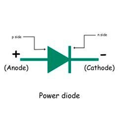
The power diode symbol is similar to low-power conventional diodes.
The “triangular shape” of the power diode denotes the Anode (A) or P-side and the straight vertical line represents the Cathode (K) or N-side.
The Anode or P is the positive terminal and Cathode or N is the negative terminal. Depending upon the biasing voltage, the power diode conducts in either direction.
Power diode working principles
The long section 3 discusses everything about power diodes supported by relevant diagrams. It explains a bit of diode theory to provide better details about power diodes. Section 3 starts with the power diode structure, and details further the working, theory, and characteristics curve. The section ends with an explanation of power diode connections to provide desirable output.
Power diode structure
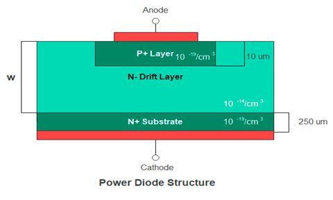
A semiconductor diode becomes a power diode upon deposition of an additional layer and adjusting the doping concentration of the structure. Power diodes have a vertical structure that increases the surface area. The vertical manufactured structure enables power diodes to dissipate more heat, withstand high power, and offer low on-state losses.
A larger area of cross-section increases the current carrying capacity of the diode. Simply put, the addition of a lightly doped drift layer is done between heavily doped layers to increase the power ratings of the device and allow for conductivity modulation. The limitation of adding the drift layer in the power diode is the increase in ohmic resistance, which in turn leads to high heat dissipation in forward bias. Hence, power diodes come with several mountings to dissipate heat.
In a power diode, the N+ substrate functions as a cathode. The N+ substrate layer has a thickness of about 250 micrometers and a carrier concentration of 1019/ cm3. The N- drift layer is epitaxially grown over the N+ substrate. The drift layer is a lightly doped N- layer of a thickness (W) of about 150 micrometers and a low carrier concentration of 1014 / cm3. It is important to note that the thickness of the N^- drift layer is subject to change as per the voltage requirements.
The heavily doped P+ layer is diffused on the N- drift layer. The P+ layer has a small thickness of about 10 micrometers, and a carrier concentration of 1019 / cm3 to function as the anode of the power diode. There is only a single junction in the diode between the P+ layer and the N- drift region called J1 or P+N-. The depletion region, or space charge region, has a high thickness and extends more into the N^- drift layer compared to the P+ layer. However, depletion region boundaries can change in power diode design and application.
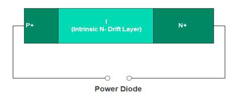
Structurally, a power diode is similar to a PIN diode. The N- drift layer is lightly doped, unlike the heavily doped N+ and P+ layers. Due to the minor doping concentration, the N- drift region can be called an intrinsic layer of the PIN diode.
Power diode working
The scope of this article is to explain power diodes. To understand power diodes, one should know the basic theory about diodes. Our article on “Diodes” explains the construction, working principles, and operation of a diode in detail.
Looking at the diode theory, a lightly doped region has a low charge carrier concentration to create a larger depletion region. As a result, the diode has a high peak inverse voltage and breakdown voltage. On the other hand, a Zener diode has a heavily doped region with a high charge carrier concentration to create a narrower depletion layer. Hence, the lightly doped layer increases the voltage handling capacity of the power diode.
Zero Bias
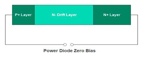
Under zero bias conditions, no current flows through the power diode. The power diode acts as an open circuit.
Forward Bias
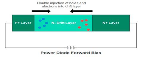
The power diode is in forward bias when the P+ layer is connected to the positive terminal, and N+ is connected to the negative terminal of the battery. Junction J1 (P+ N-) becomes forward-biased. Holes from the P+ layer are injected into the N- drift layer. As the N- drift layer is lightly doped, the carrier concentration is less in the region to initiate electron-hole recombination. The excess holes in the N- drift layer attract electrons from the N+ region. Again, electrons are injected into the N- drift layer. The process where holes from the P+ layer and electrons from the N+ region are injected into the N^- drift layer is called double injection.
The number of electrons and holes becomes equal in the N- drift layer. As discussed above, the increase in carrier concentration decreases the depletion region width. In conclusion, the resistance decreases, and current flow increases in the power diode. The resistance of the N- drift layer eventually becomes constant.
Reverse Bias
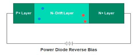
When the power diode is in reverse bias, the N+ layer is connected to the positive terminal, and the P+ layer is connected to the negative terminal of the battery. Junction J1 (P+ N-) becomes reverse biased. Holes from the P+ layer are not injected into the N- drift layer due to the negative attractive force on the P+ terminal. Similarly, electrons in the N+ layer repel the N- drift layer because of the attractive positive voltage at the N+ region. This decreases the charge carrier concentration in the depletion region. As a result, the depletion region width becomes wider to increase the resistance of the power diode.
Ideally, the power diode is designed to block the current flow in reverse bias mode. However, a small undesirable leakage current flows in the opposite direction to the forward current in the diode. The leakage current may arise through thermal generation of minority carriers, or manufacturing defects. When the reverse voltage exceeds the breakdown voltage value, the electric field accelerates the charge carriers to gain high kinetic energy, and collide with other particles.
The impact ionization process states that the collision between high-energy charge carriers and other atoms in the power diode knocks electrons from the bonded atom or generates electron-hole pairs. The process of impact ionization leads to the rapid multiplication of charge carriers that contribute to reverse current. This effect is known as avalanche breakdown in power diodes. Impact ionization and avalanche breakdown are cyclic processes that heavily increase reverse current.
:quality(80):fill(efefef,0)/p7i.vogel.de/wcms/65/69/6569f9912322b/202312-whitepaper-ametek-coverbild.png)
Power diode theory
This subsection explains two important concepts of conductivity modulation and reverse recovery time in power diodes. These two parameters decide the performance of the power diode in the target application.
Conductivity modulation
Conductivity modulation is an important factor in power diodes to improve performance and increase the efficiency of power electronics systems. The practical value of the on-state resistance of the N- drift layer is much lower than the estimated value. The reason for the low on-state resistance of the drift region is conductivity modulation. As the name suggests, conductivity modulation is the process of increasing conductivity or reducing the resistivity of the drift region under a set of conditions. The conductivity modulation is achievable only during forward bias (conducting mode).
As discussed above, excess charge carriers are injected into the N- drift layer. Holes from the P+ layer and electrons from the N+ region are double-injected into the N- drift layer. The increased carrier concentration decreases the resistance of the depletion layer. Furthermore, the power diode current increases but the resistance of the drift region remains constantly low. Conductivity modulation is defined as an intentional increase in conductivity of the N- drift layer due to excess charge injection by heavily doped N+ and P+ layers into the N- drift layer.
The result of conductivity modulation is the decrease of on-state voltage drop, on-state power dissipation, fast switching speed, and enhanced dynamic characteristics.
Reverse recovery time
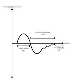
Reverse recovery time is the time taken by a power diode to transition from the conducting mode in forward bias to the blocking state in reverse bias. The power diode takes some time to become non-conductive in the reverse bias. Even in reverse bias, the power diode is conductive for a small time period.
Simply put, reverse recovery time is the time taken by the power diode to stop conducting upon the application of polarity change to reverse bias. The end result of reverse recovery time is zero current flow in the power diode. Reverse recovery period is a natural behavior of any semiconductor device.
As explained, forward current increases exponentially when the input voltage exceeds the on-state voltage. When the diode switches from forward bias to reverse bias, the current decreases slowly and doesn’t turn zero abruptly. The stored charge carriers (minority carriers) in the depletion region take a small time to recombine. Moreover, an undesirable small leakage current flows in reverse bias.
Reverse recovery time can be defined as the time period between the instant at which the forward current reaches zero and another instant at which the reverse leakage current decays up to 25 % of peak reverse value. Reverse recovery time is considered important at the time of switching when the power diode transitions from forward conducting mode to reverse blocking mode.
The reverse recovery period of a power diode depends upon:
- Value of forward voltage and forward current.
- Storage time.
- Transit time.
- Charge removal time.
- Reverse recovery charge.
- Junction capacitance.
- Load.
Storage Time: The storage time is defined as the time taken by the stored charge or minority carriers from the depletion region to recombine. In simple words, storage time is the time period for which a power diode remains conducting in reverse bias.
Transit Time: Transit time is defined as the time taken by the power diode to become non-conductive in the reverse bias.
Charge Removal Time: The time taken to remove the stored charge from the junction and establish the reverse-biased condition.
Reverse recovery charge: Reverse recovery charge is the number of charge carriers that flow towards the reverse direction upon application of reverse bias. If electrons flow from the cathode to the anode in forward bias, the same electrons start to move from the anode to the cathode in reverse bias.
Hard recovery and soft recovery: Power diodes have two types of reverse recovery time periods- hard recovery and soft recovery. Hard recovery is the process where the power diode rapidly transitions from the conducting state to the blocking state but takes a longer transition time. In simple words, hard recovery has a high reverse recovery time and high switching losses. Soft recovery is another process in power diodes that offers a smooth transition from the conducting state to the blocking state in a short time.
Why is a power diode an uncontrolled power device?
An uncontrolled power device does not allow the user to have control over the switching process. The user cannot control the transition between the on and off states. In a power diode, the external signal cannot control the transition between conducting and blocking states. The power diode conducts only in one direction and blocks the current flow in the other direction based on the input voltage. In simple words, a user cannot switch on and off an uncontrolled power device. Hence, power diodes are uncontrolled devices that cannot be turned on and off by the user.
Power diode characteristics
The ideal characteristics of a power diode are somewhat similar to those of low-power diodes. Power diode ideal characteristics are not enough to estimate converter topology and design. The voltage required to turn on a semiconductor device is called the on-state voltage or forward voltage drop. The forward voltage drop of low-power diodes is about 0.7 V for Silicon and 0.3 V for Germanium-based diodes.
The forward voltage for power diodes is 1 V, which is much higher than the conventional diodes. The reason for the higher forward voltage drop is the presence of the N^- drift layer. The low carrier concentration increases the resistance of the power diode. When the input voltage exceeds the forward voltage drop or on-state voltage, the forward current increases exponentially. There is a high ohmic drop that turns the voltage-current relationship almost linear in the forward blocking mode. However, the voltage-current relationship is not completely linear in the characteristics.
In reverse bias, a small leakage current flows through the device. The undesirable leakage current is independent of input reverse voltage. Once input reverse voltage exceeds breakdown voltage, avalanche breakdown occurs in the power diode. The breakdown voltage of a power diode is dependent upon the doping profile of the junction and carrier concentration. When avalanche breakdown occurs, reverse current heavily increases. The power diode is not designed to dissipate such a large amount of heat and the device can get damaged.
Power diode connections
Most power diodes are connected in series or parallel, depending upon the application. A single power diode may not be able to meet high power requirements in a power electronic system. Hence, many power diodes collectively contribute to power electronic system efficiency.
Power diodes in series
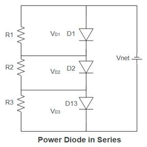
Power diodes are connected in series to provide higher voltage ratings and increase the reverse blocking capabilities in power electronic systems. The total voltage across the power diode circuit is the addition of the contribution of each power diode’s voltage. In the figure below three diodes (D1, D2, and D13) and three resistors (R1, R2, and R3) are connected. The three diodes are connected in series. VD1 is the voltage across diode D1, V2 is the voltage across diode D2, VD3 is the voltage across diode D13, and Vnet is the total voltage of the circuit.
In forward bias, each diode shares the total voltage equally. This is because each diode conducts the same amount of current and has the same voltage drop. However, diodes have different blocking voltages in reverse bias. To increase the reverse blocking capability, it is important to connect resistors in the circuit.
Power diodes in parallel
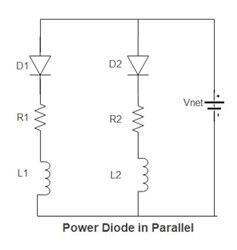
Power diodes with the same forward voltage drops are connected in parallel to provide higher current ratings. Resistors are connected in the circuit for current sharing in steady-state conditions. Under dynamic conditions, coupled inductors are connected in the circuit. In the figure below two diodes (D1 and D2), two resistors (R1 and R2), and two inductors (L1 and L2) are connected. Vnet is the total voltage of the circuit.
The diagram shows the dynamic sharing of the current. When the current in D1 increases, emf is induced in L1. By electromagnetic induction, an opposite polarity voltage is induced in L2. The total current across the power diode circuit is the addition of the current handling capacity of a single diode. In simple words, each diode shares the total applied current uniformly.
:quality(80):fill(efefef,0)/p7i.vogel.de/wcms/65/5c/655c87f111972/202311-whitepaper-tektronix-coverbild.png)
Power diode types
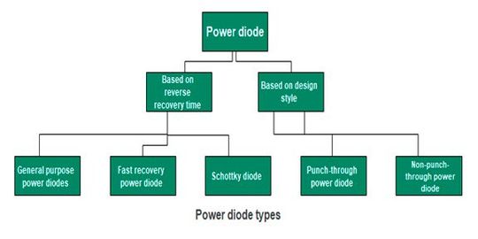
The requirements of the reverse recovery time, feature design, and voltage and current ratings along with other characteristics in the projects categorize power diode types. The article lists five types of power diodes based on two classifications.
Classification 1: Power diode types based on design features
The main emphasis of design feature classification is the position of the depletion layer in power diodes. The depletion layer width is a deciding factor in the power diode’s forward and reverse operation with the characteristic curves. The classification based on design features creates two different types of power diodes.
Punch-through power diode (PT)
A punch-through power diode is used in applications that require fast switching. The depletion region of a punch-through power diode spans into the N- drift layer and extends into the N+ cathode. A PT-power diode has a lower temperature coefficient and depletion layer resistance.
Classification 2: Power diode types based on reverse recovery time
There are many types of power diodes available in the market based on reverse recovery time and associated applications. General purpose power diodes, fast power recovery diodes, and Schottky diodes are power diode types listed in the order of reducing reverse recovery time.
Standard power diode
A standard power diode, also known as a power frequency diode or general purpose diode, is the most common power diode available in the market. Standard power diodes have a high power rating, low cost, high voltage rating from 50 V to 5 kV, and high current rating from 1 A to 1 kA. The drawback associated with standard diodes is the high reverse recovery time of up to 30 microseconds.
General-purpose diodes are not applicable in time-specific and high-frequency applications due to high reverse recovery time. General-purpose diodes are used in converters, rectifiers, battery chargers, SMPS, and many more high-power applications.
Fast recovery power diode
Power fast recovery diodes are an advancement of general-purpose power diodes. The reverse recovery time of these diodes ranges from 2 to 5 microseconds and the power rating is from 50 V to 3 kV. To achieve a lower reverse recovery time, power diodes are doped either with platinum or gold.
Gold dopants are costlier than the entire cost of the project. Doping the power diode with gold/platinum dopants was a proposed device in the 1960s. Such devices may also increase the forward voltage drop of the power device. Power-fast recovery diodes are used in choppers, DC-DC converters, SMPS, etc.
Schottky diode
In our detailed article, we have covered Schottky's diode operation, working principles, and applications. A Schottky diode has a metal-semiconductor junction, in which the semiconductor could either be P or N-type. The discontinuity in the metal-semiconductor junction and the fermi level misalignment gives rise to a potential Schottky barrier.
As there is no space for storing charge carriers, Schottky diodes theoretically have a zero reverse recovery time. Practical Schottky diodes in power electronics have a reverse recovery time of less than one microsecond. Schottky diodes are used in high current-low voltage power rectifiers, clamp diodes, RF mixers, detectors, and high-frequency switching power supplies.
Power diode applications in power electronics
Power diode applications in power electronics include:
- Battery charging and discharging in electric vehicles.
- Power rectification.
- A power diode is a feedback diode in inverters.
- Snubber circuit.
- Feedback diodes.
- DC power supplies.
- Choppers.
- SMPS.
- Induction heating.
Flyback power diode
Power diode is used as a Flyback diode in inductive loads. At zero instant, the current flows through the circuit. When the switch is turned off, the current does not become zero abruptly. The current slowly decays in the circuit. The inductor resists the change and generates a back EMF, a large voltage spike, proportional to the value of L di/dt across the circuit. The large voltage spike could potentially damage other components in the circuit. The Flyback diode bypasses the large voltage spike through a controlled path for the inductive current flow.
Power diode advantages
Power diodes offer several advantages that make them highly valuable in power electronic applications, including their ability to handle high voltage and current with reliability and efficiency.
- A power diode is a large signal device.
- Power diodes have high voltage and current ratings, making them serve many power electronic applications.
- Power diodes can pass high currents in the kiloamperes at a high voltage with negligible power dissipation.
- Power diodes can block high kilovolts reverse voltage.
- Modern power diodes have low forward voltage drops.
- Some power diodes like Schottky diodes and fast recovery power diodes have low reverse recovery time.
- Power diodes can operate at high temperatures.
- Power diodes have a simple design, and are reliable and cost-effective.
Power diode disadvantages
Despite their benefits, power diodes also come with a set of disadvantages that must be considered, particularly their potential for high power dissipation and size constraints within circuit designs.
- High voltage and current ratings can cause high power dissipation.
- Power diodes can get damaged during reverse breakdown.
- Power diodes are larger in size and require heat sinks to cool them down.
- Voltage spikes occur in power diodes.
- Common types of power diodes generally have a higher reverse recovery time.
- Power diodes have high junction capacitance.
- Fast recovery power diodes can trigger a transient in the circuit.
Power diode vs conventional diode
In contrast, the significant difference between low-power semiconductor diodes and high-power devices is the drift layer, vertically oriented structure, and nature of breakdown. Power diodes usually have high recovery times. In fact, most power devices have low switching frequency but high power ratings. At the same time, low-power diodes have high switching frequencies and much lower ratings.
| Parameter | Conventional Diode | Power Diode |
|---|---|---|
| Number of doped layers | Two: N+ and P+ | Three: N+, N-, and P+ |
| Type | Small signal device | Large signal device |
| Drift layer | Absent | Present |
| Breakdown | Zener or Avalanche | Avalanche |
| Structure | Horizontally-oriented | Vertically oriented |
| Power rating | Low | High |
| Voltage rating | Low | High |
| Current rating | Low | High |
| Switching speed | High | Low |
| Applications | Low power rectification | High-power devices, the freewheeling diode in inductive loads, and power supplies |
(ID:49848610)


:quality(80)/p7i.vogel.de/wcms/55/5b/555bb8759d60243792dd736b86585f29/0130909253v2.jpeg)
:quality(80)/p7i.vogel.de/wcms/db/75/db7507346cd4842ca5eb8838f45861ce/0130908924v2.jpeg)
:quality(80)/p7i.vogel.de/wcms/44/0f/440f92984dc6c58eec920824ef55b54c/0130740285v2.jpeg)
:quality(80)/p7i.vogel.de/wcms/be/dc/bedc263ae2b17f59ef71bfc822b95d27/0130740269v2.jpeg)
:quality(80)/p7i.vogel.de/wcms/ea/60/ea600a89db0dc673ba3b6eb1ca56093e/0130736129v2.jpeg)
:quality(80)/p7i.vogel.de/wcms/8b/ae/8bae28ce8ab5e6820bc036ce49939261/0130655531v2.jpeg)
:quality(80)/p7i.vogel.de/wcms/de/9b/de9beb17c1467fdb18301a114f31bf8e/0130651681v2.jpeg)
:quality(80)/p7i.vogel.de/wcms/47/47/474773560a05ff45872e5942c2702e11/0130617850v2.jpeg)
:quality(80)/p7i.vogel.de/wcms/07/89/0789a27b7dcc43dbdafd17f2b601e3a7/0130908474v2.jpeg)
:quality(80)/p7i.vogel.de/wcms/9e/b0/9eb01567f828f28e7922897edc690be2/0130454119v2.jpeg)
:quality(80)/p7i.vogel.de/wcms/db/bb/dbbb1b9c429bd4fc375a7937bb083ba1/0130804041v2.jpeg)
:quality(80)/p7i.vogel.de/wcms/a3/30/a330337e234ac2000bb8829ce34ce001/0130871678v2.jpeg)
:quality(80)/p7i.vogel.de/wcms/34/4a/344a3dc5a19429cf6726b7f8f7e2ee32/0130109719v2.jpeg)
:quality(80)/p7i.vogel.de/wcms/be/c8/bec8d43fc0ee73414274be44608b2970/0129748903v2.jpeg)
:quality(80)/p7i.vogel.de/wcms/23/ee/23ee4a97790d6009dbfd7d9577ffa723/0129220424v2.jpeg)
:quality(80)/p7i.vogel.de/wcms/3c/d1/3cd1cacbceb792ba63727199c61ca434/0127801860v2.jpeg)
:fill(fff,0)/p7i.vogel.de/companies/63/c7/63c7da97be945/diotec.png)
:fill(fff,0)/p7i.vogel.de/companies/62/a0/62a0a0de7d56a/aic-europe-logo.jpeg)
:fill(fff,0)/p7i.vogel.de/companies/5f/71/5f71d5f92a5f6/2000px-rogers-corporation-logo-svg.png)

:quality(80)/p7i.vogel.de/wcms/af/07/af073e302fcca1153bcaca553175006c/0124143921v2.jpeg)
:quality(80)/p7i.vogel.de/wcms/8b/ed/8bed230f3f9de9859f94928062984cec/0124637555v2.jpeg)