Semiconductor Material Gallium oxide: Hidden gem
Related Vendors
Suppose three friends gear up to replace the most popular kid in the school. That’s what Silicon Carbide (SiC), Gallium Nitride (GaN), and Gallium Oxide try to do with Silicon. While SiC and GaN were successful in reducing silicon dominance to a certain extent, gallium oxide is less well-known. However, gallium oxide is a compound semiconductor that is cheaper and easier to manufacture.

Gallium Oxide as a Semiconductor
Gallium oxide is a metal oxide. The research to expand the capabilities of this inorganic compound semiconductor has continued for 70 years. The section explains its unique properties that differentiate it from other wide bandgap semiconductors such as GaN, SiC, and even the latest AIN (Aluminum Nitride).
Structure
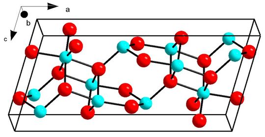
The chemical formula for gallium (III) oxide is Ga2O3. Gallium forms an ionic bond with oxygen, slightly showcasing covalent characteristics. Each gallium atom loses three electrons to oxygen, and each oxygen gains two electrons. Gallium oxide has three types of crystalline structures, with the most common β, followed by ε and α . β-Gallium oxide is the most stable of them all at standard temperatures and pressures.

Wide band gap
Gallium oxide is an ultra-wide bandgap (UWBG) semiconductor, having a bandgap energy of 4.8-4.9 eV, higher than SiC and GaN. Having a wide bandgap means that more energy is needed to knock off electrons from the lower energy band to move freely in the upper energy band. A UWBG semiconductor exhibits an increased breakdown field. As a result, gallium oxide exhibits a high breakdown field and operates at high voltages.
Standard fabrication compatibility
Ga2O3 is manufactured to be a semiconductor. Compared to other UWBG oxides such as aluminium oxide, zinc oxide, and magnesium oxide, gallium oxide is easier to manufacture. These oxides are not compatible with standard ion implantation doping procedures. Ga2O3 can tolerate dopants without destroying the structure. It is also compatible with silicon-like fabrication, lithographic, and etching processes, making it cheaper to manufacture.
:quality(80)/p7i.vogel.de/wcms/8d/e0/8de08e7cf8c954f00d30a4a1894a8294/0126807438v2.jpeg)
COMPARISON
Battle of SiC vs GaN power modules
Wafer manufacturing
Gallium oxide crystals can even grow from the melt. Ga2O3 is compatible with the Czochralski crystallization method. Hence, large gallium oxide single-crystal bulks can be manufactured in high volumes. Gallium oxide wafers are large in size and lower in cost than GaN and AIN wafers. In addition, Ga2O3 can also function as its own wafer; it doesn’t need Si like GaN on Si or SiC on Si. However, Gallium oxide on SiC has been developed in the US.
Where does Gallium Oxide lack?
Gallium oxide did not turn out to be as applicable as SiC and GaN due to three major reasons.
- 1. Quick heating : One of the drawbacks of Ga2O3 is its low thermal conductivity of 10 W/m-k. Now we know why gallium oxide doesn’t win the race with SiC and GaN. Thermal conductivity is the ability of materials to spread heat through their bodies. A low thermal conductivity shows that gallium oxide quickly heats up, requires intensive heat management, and becomes unsuitable for SiC and GaN levels of power electronics applications.
- 2. No p-type: β-Ga2O3 is a promising n-type semiconductor, but manufacturing a p-type semiconductor using it is not possible. It is a major drawback as p-type semiconductors are important in various applications. The reason is the metal oxide’s internal structure. The electron mobility of gallium oxide is not very good, but is still “okay”, while the hole mobility is extremely poor, lower than 1 cm^2/V.s.
- 3. Lack of availability Gallium oxide semiconductors are not as easily available as their Si, SiC, and GaN counterparts. The reason is simple - demand and supply. The demand for gallium oxide in manufacturing power diodes and transistors is limited. As a result, the supply is less. The commercial gallium oxide wafers exist at 2 inches, less than the industrial standards.
Gallium Oxide applications and initiatives
Some companies are formed only for gallium oxide research, commercialization, and manufacturing. It is applicable due to its cost-effectiveness and some unique features. The section lists some gallium oxide commercial applications and recent initiatives.
:quality(80)/p7i.vogel.de/wcms/e1/03/e1037c01bbe9722bf96e292e0010bbbe/0125512618v2.jpeg)
GALLIUM NITRIDE
What is a GaN charger and is it safe for use?
- Optoelectronics: Beta-Ga2O3 has an indirect band gap. It means the valence and conduction bands are not at the same momentum. However, the direct and indirect band gaps of Beta-Gallium oxide are very close in energy. Beta-Gallium oxide is suitable for absorbing UV light and functioning for light emission purposes. Examples include deep-UV detection (DUV), solar-blind UV photodetectors, LEDs, lasers, and luminescent applications.
- Space electronics: Researchers predict that Beta-Gallium oxide is radiation-hard, meaning it offers resistance to radiation better than most third-generation semiconductors. As a result, it may be applicable in space applications.
- Power electronics: Even with poor thermal performance, gallium oxide multi-kV power transistors - MOSFETs and JFETs, power diodes, Schottky diodes, and gas sensors are available in the market.
- Radio frequency (RF): Gallium oxide is a tunable semiconductor. It is applicable in RF power devices such as HEMTs, MESFETs, RF switches, mixers, and RF power detectors.
- Energy management: Gallox Semiconductors, a company dedicated to producing gallium oxide diodes and transistors, is reducing energy waste through efficient power conversion.
- Iridium gallium oxide: Two Japanese companies have recently developed an iridium-based thin film for Ga2O3 semiconductor, now called Iridium gallium oxide.
- 6-inch wafers: Japanese company specialising in Ga2O3 wafers. The company, known for its 2-inch gallium oxide wafers, is all set to mass-produce 6-inch gallium oxide wafers in 2026.
- Gallium oxide heterostructures: In Germany, a project named "All-GO-HEMT" has received funding of 2 million euros to develop aluminum-alloyed gallium oxide heterostructures. Led by a German R&D enterprise, the researchers aim to solve low carrier mobility problems in Ga2O3 semiconductors.
(ID:50622929)


:quality(80)/p7i.vogel.de/wcms/55/5b/555bb8759d60243792dd736b86585f29/0130909253v2.jpeg)
:quality(80)/p7i.vogel.de/wcms/db/75/db7507346cd4842ca5eb8838f45861ce/0130908924v2.jpeg)
:quality(80)/p7i.vogel.de/wcms/44/0f/440f92984dc6c58eec920824ef55b54c/0130740285v2.jpeg)
:quality(80)/p7i.vogel.de/wcms/be/dc/bedc263ae2b17f59ef71bfc822b95d27/0130740269v2.jpeg)
:quality(80)/p7i.vogel.de/wcms/ea/60/ea600a89db0dc673ba3b6eb1ca56093e/0130736129v2.jpeg)
:quality(80)/p7i.vogel.de/wcms/8b/ae/8bae28ce8ab5e6820bc036ce49939261/0130655531v2.jpeg)
:quality(80)/p7i.vogel.de/wcms/de/9b/de9beb17c1467fdb18301a114f31bf8e/0130651681v2.jpeg)
:quality(80)/p7i.vogel.de/wcms/47/47/474773560a05ff45872e5942c2702e11/0130617850v2.jpeg)
:quality(80)/p7i.vogel.de/wcms/07/89/0789a27b7dcc43dbdafd17f2b601e3a7/0130908474v2.jpeg)
:quality(80)/p7i.vogel.de/wcms/9e/b0/9eb01567f828f28e7922897edc690be2/0130454119v2.jpeg)
:quality(80)/p7i.vogel.de/wcms/db/bb/dbbb1b9c429bd4fc375a7937bb083ba1/0130804041v2.jpeg)
:quality(80)/p7i.vogel.de/wcms/a3/30/a330337e234ac2000bb8829ce34ce001/0130871678v2.jpeg)
:quality(80)/p7i.vogel.de/wcms/34/4a/344a3dc5a19429cf6726b7f8f7e2ee32/0130109719v2.jpeg)
:quality(80)/p7i.vogel.de/wcms/be/c8/bec8d43fc0ee73414274be44608b2970/0129748903v2.jpeg)
:quality(80)/p7i.vogel.de/wcms/23/ee/23ee4a97790d6009dbfd7d9577ffa723/0129220424v2.jpeg)
:quality(80)/p7i.vogel.de/wcms/3c/d1/3cd1cacbceb792ba63727199c61ca434/0127801860v2.jpeg)
:fill(fff,0)/p7i.vogel.de/companies/63/c7/63c7da97be945/diotec.png)
:fill(fff,0)/p7i.vogel.de/companies/66/8b/668becd1c07eb/dowa-logo-word--1-.jpeg)
:quality(80)/p7i.vogel.de/wcms/7d/40/7d406bd959b3a9127c33a66157f9030a/0128339184v4.jpeg)
:quality(80)/p7i.vogel.de/wcms/8d/e0/8de08e7cf8c954f00d30a4a1894a8294/0126807438v2.jpeg)