SILICON CARBIDE Double-Pulse test helps validating SiC SPICE models
Related Vendors
When simulating complicated switching converters like 3-phase PFCs, you want to ensure the selected SPICE models of the SiC transistors are doing the right job. There is nothing more frustrating than a long simulation ending with wrong waveforms because the models were bad. This article shows how a simple double-pulse test can let you check if a given SPICE model is faithfully matching the data-sheet parameters or, on the contrary, needs to be replaced by another subcircuit model.

When analyzing complex structures with a simulator, I always start with a simplified circuit that I exercise to verify my approach is correct. For instance, if I need a power element such as a MOSFET, I will first use a voltage-controlled switch, verify it performs as expected and then, insert a real model if need be. Similarly, for a compensator, I may first resort to a simplified operational amplifier subcircuit then verify the overall ac response is adequate, before dropping-in a more comprehensive commercial model. This approach helps me safely assemble the final circuit by confirming that the last block I have added simulates seamlessly otherwise, it must be fixed.
This step-by-step implementation is important when you run simulations of several tens of minutes – sometimes longer as with a power factor correction (PFC) circuit – because you do not want to realize, in the end, that your waveforms are wrong because of a poorly-tested subcircuit or model. That is exactly what I did when recently working on a three-phase active power factor correction circuit whose purpose was to check the power dissipation budget for all switching elements: voltage-controlled switches were acceptable for debugging the circuit but in the end, a good, realistic model is needed. The double-pulse test offers an interesting way to verify the accuracy of the selected model and this short article explains how it works.
Energizing an inductor
Figure 1 shows a simple circuit involving an inductor, a diode and a power switch. The inductor model includes an equivalent series resistance rL but I did not show it for simplicity. When the power switch turns on for a ton duration, the input source Vin appears across the inductor if we neglect the voltage drop of the switch. If we now consider the time constant L/rLvery large compared to the on-time, then the current ramps up with a slope expressed in [A]/[s] equal to equation 1.

When the switch turns off and assuming a 0-A initial current condition in the circuit, the inductor current will peak as shown in equation 2.

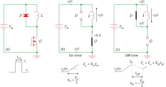
When the switch opens, the inductive current keeps circulating in the same direction but now finds a path or freewheels in diode D. The voltage across the inductor reverses, reducing the current with a slope defined by equation 3.
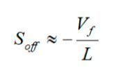
In this expression, Vf represents the forward voltage of the diode at the considered peak current. If the switch remains open long enough, the current decreases to a valley point determined as seen in equation 4.

If the switch is turned back on again at Iv, the current ramps up again as defined by (1) and the inductor current is said to be continuous. On the contrary, if the inductor would totally deplete considering a long off-time, then the valley current would be zero and the conduction mode be discontinuous.
:quality(80):fill(efefef,0)/p7i.vogel.de/wcms/5f/fe/5ffedb2e0ffa6/listing.jpg)
A brief short circuit
As long as the inductor is energized, the diode freewheels the current and the voltage at the drain node is equal to Vin + Vf. If you now turn Q back on while the diode conducts, you brutally reverse the voltage across D in an attempt to block it: the current decreases with a slope now dependent on the stray inductance present in the circuit (PCB traces, bonding wires etc.) and the transistor turn-on speed. The classical idealized current shape is shown in Figure 2.
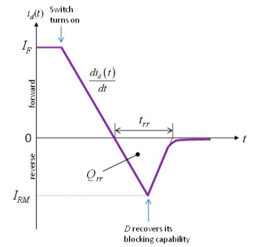
As the diode blocking mechanism is started, the current decreases quickly and when it passes below zero, it reverses direction, making the diode behave as a short circuit. This reverse current overshoots and peaks at IRM. This value depends on the junction temperature and the turn-off slope imposed by the external elements. For instance, slowing down the low-side transistor Q is a known means to affect the current downslope. When the current reaches IRM, the diode has recovered its blocking capability and the current reduces towards a leakage value with a shape also depending on various parameters. The charge recovered during this period of time trr is denoted Qrr and expressed in coulombs. The loss incurred by this hard-switching event affects the diode but also the switch as it undergoes the current spike. Going into the details of this phenomenon is beyond the scope of this short article but Ref. [1] nicely documents the various aspects of this operating mechanism.
Hard-switching happens in PFCs operated in continuous conduction mode (CCM) and designers can use SiC diodes in high-power designs as they exhibit a negligible reverse recovery charge. In motor control applications, hard-switching occurs because the body diode of the upper transistor freewheels the inductive current during deadtime and brutally blocks when the low-side transistor conducts again. A high current circulates which affects losses, reliability and the electro-magnetic interference (EMI) signature too as these narrow energetic spikes flow in loops and radiate energy. Proper modeling of the diode and the transistor are therefore important if you want to trust your simulation results. One way to verify the model approaches reality is to reproduce the double-pulse test.
:quality(80)/images.vogel.de/vogelonline/bdb/1787400/1787413/original.jpg)
SILICON CARBIDE
Silicon carbide market size worth $79.0 million by 2027
Double-Pulse test
This test is an industry standard used by manufacturers to characterize their power components during a hard-switching event. It can be used to check a discrete diode performance or the body diode of a transistor when freewheeling inductive current in the third quadrant. The reader interested by this technique can read the article from Ref. [2] which details the various possible configurations. A typical circuit is shown in Figure 3. The left-side picture represents the circuit simulated with SIMetrix SPICE while the right one illustrates an LTspice electrical schematic.
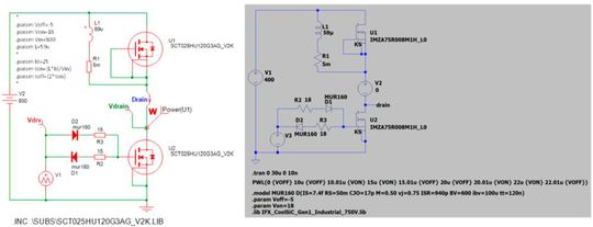
Since you want to reproduce a CCM operation, you first energize the inductor by actuating the low-side transistor and have the current reach the level given in the data-sheet of the considered component, e.g. 25 A in this example. The transistor is then turned off to let the current freewheel in the upper-side diode. After a few micro-seconds, you turn the low-side switch back one again to block the diode and observe the reverse-recovery effects. What you want to assess is the loss in the low-side power transistor produced by the recovery of the diode. In this example, the two transistors are the same part, like in a half- or full-bridge configuration. But you could also insert a diode model and check the switching performance to reproduce the switching cycle of a CCM PFC for instance.
It is important to underline that this is a simplified circuit in the sense that I have not purposely included all the parasitics which are part of the practical implementation in your converter: the dc bus output impedance, the stray inductance in the gate drive path, the bonding inductances, the parasitic capacitors (many are nonlinear) or the distributed ohmic losses. Some of these contributors are part of the power distribution network (PDN) and affect the switching performance. Careful parameters extraction is thus key if you want realistic results with your models. References [3] and [4] offer additional information on the importance of these parasitics.
When running this simulation, you will need to duplicate the basic test conditions given in the data-sheet like gate resistance, inductive current and control voltage. The below table shows what the data-sheet of the SCT025HU120G3AG, a 1200-V, 27-mOhm SiC transistor from ST states:

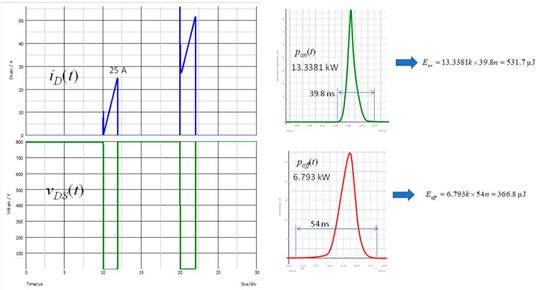
The on-time will be adjusted via (2) to meet the peak current during the first pulse. The depletion rate of the inductor is slow and you can wait another few micro-seconds before actuating the low-side switch, it will not significantly impact the valley current. When running Figure 3’s circuit in SIMetrix, you obtain the waveforms of Figure 4. Multiply the drain voltage with the current in the low-side transistor and you have the instantaneous power p(t). Zoom-in the turn-on or turn-off sequence of the second pulse and carefully place cursors on both sides of the pulse. Average the waveform between the cursors (you obtain kW) and multiply by the pulse width to end up with joules. In this example, the energy lost at turn on is a bit off compared with the data-sheet and it could be explained by the strong
IRM value of the body diode while recovering. Keep in mind that I do not have parasitic inductances in my simulation circuit and the di/dt is probably very large when the low-side transistor turns on. The off transition is not far away from the data-sheet number and the model looks like a valid candidate for assessing losses, again as crude results as it is extremely difficult to simulate switching losses in absence of the comprehensive characterization of the power distribution network, including the drive path.
The simulation with LTspice also gives good results and inserting a SiC model from Infineon is simple by linking the library file with a .LIB statement. Make sure the maximum time step is purposely reduced to a few nano-seconds (e.g. 5 ns) so that you obtain adequate resolution for plotting the waveforms and analyzing them. Same principle here, zoom-in and isolate the second power pulse transition on the screen. While pressing the control key, left-click with the mouse on the waveform name and the integrated result appears in joules.

More comprehensive models can be tested like those computing the junction temperature and case, with dynamic effects on switching parameters. If they are extremely precise, they tend to overload the simulation engine and the simulation of large circuits like 6-pack PFC becomes impractical in my opinion. My recommendation is to simulate with perfect switches first, then drop your transistors SPICE models (MOSFET, SiC or GaN) for an estimation of conduction and switching losses, keeping in mind that the absence of thorough characterization of the PDN leads to imprecise values. In the end, bench measurements rule!
:quality(80)/p7i.vogel.de/wcms/48/32/4832baab84aba8e9100a6dc122eabb36/0115792955.jpeg)
TRANSISTOR TYPES
Different transistor types and features
Conclusion
The simulation of electronic circuits often requires to find the right balance between models’ complexity, convergence and simulation time. Using perfect elements to quickly validate a design is a sound approach but if switching losses or complex transition mechanisms need to be observed, it is best to resort to real models. However, when simulation time is already long because of the nature of the circuit – a PFC for example – you cannot afford to waste hours to finally discover that your transistors models are bad. Testing the subcircuit in a dedicated setup like what has been presented in this article, represents a possible way to validate a given model before implementing it in your simulation circuit.
Reference
- 1. O. Vogt et al., Diode Application Handbook, Fundamentals, Characteristics, Applications, NEXPERIA, May 2022
- 2. D. Levett, Z. Zheng, T. Frank, Double Pulse Testing: The How, What and Why, Bodo’s Power Systems, April 2020
- 3. Double Pulse Testing: The How, What and WhyWolfspeed Power Module SPICE Models User Guide, PRD-07913, Wolfspeed, December 2023
- 4. Discrete Double Pulse Tester – Evaluation User’s Manual, EVBUM2897G-EVB, onsemi, August 2024
(ID:50316080)


:quality(80)/p7i.vogel.de/wcms/2f/f3/2ff3221bf7665de2d0acf83760bfd1fa/0130031523v2.jpeg)
:quality(80)/p7i.vogel.de/wcms/c3/16/c316e955a97f5d72d9678297b237b9e5/0129932858v2.jpeg)
:quality(80)/p7i.vogel.de/wcms/ef/0a/ef0adb0acf793fe147cc27c21f6a7a67/0129954238v2.jpeg)
:quality(80)/p7i.vogel.de/wcms/53/f9/53f9301dfc9292d02960f7996c79cc6e/0129927601v2.jpeg)
:quality(80)/p7i.vogel.de/wcms/6e/cd/6ecd41d095d5111cf4ed37b714844487/0129930878v2.jpeg)
:quality(80)/p7i.vogel.de/wcms/02/c0/02c0e9722f70b1134dbf96fb59a9c73d/0129655179v2.jpeg)
:quality(80)/p7i.vogel.de/wcms/cc/67/cc670ea2029cd2af5c641af70e1bf734/0129816392v4.jpeg)
:quality(80)/p7i.vogel.de/wcms/ea/e6/eae6aee30071e67a5627027974437134/0129544613v2.jpeg)
:quality(80)/p7i.vogel.de/wcms/b1/5e/b15ee02b0ba02db70cf61e37d66ad1d3/0129349127v2.jpeg)
:quality(80)/p7i.vogel.de/wcms/26/d5/26d591cc340077026eac56a0e7564faf/0129949603v2.jpeg)
:quality(80)/p7i.vogel.de/wcms/4d/e0/4de02f76a37cbb3df30dd231de589c8e/0128866890v2.jpeg)
:quality(80)/p7i.vogel.de/wcms/18/0b/180b7b63afc91e523592d8a5ce161c96/0129847487v2.jpeg)
:quality(80)/p7i.vogel.de/wcms/be/c8/bec8d43fc0ee73414274be44608b2970/0129748903v2.jpeg)
:quality(80)/p7i.vogel.de/wcms/23/ee/23ee4a97790d6009dbfd7d9577ffa723/0129220424v2.jpeg)
:quality(80)/p7i.vogel.de/wcms/3c/d1/3cd1cacbceb792ba63727199c61ca434/0127801860v2.jpeg)
:quality(80)/p7i.vogel.de/wcms/5a/a0/5aa0436498af618297961fd54ab36cdf/0126290792v2.jpeg)
:quality(80)/thumbor.vogel.de/mguFAwuAxCGw9kVi3c_k2-HNi5I=/500x500/p7i.vogel.de/wcms/66/74/667444027a724/tof1.jpeg)
:fill(fff,0)/p7i.vogel.de/companies/63/c7/63c7da97be945/diotec.png)
:fill(fff,0)/p7i.vogel.de/companies/60/7e/607ec89d5d9b5/white-frame.jpg)
:fill(fff,0)/p7i.vogel.de/companies/69/a8/69a8093b1b5e1/hvp-png.png)
:quality(80)/p7i.vogel.de/wcms/37/64/376449c482d7bc5493c77d057638fe59/0126287882v2.jpeg)
:quality(80)/p7i.vogel.de/wcms/d9/64/d964e7b776e5905b69d15374f8b8990b/0115795833.jpeg)