


:quality(80)/p7i.vogel.de/wcms/40/62/4062c2d596e53b038e0f05f6c3182509/0133843963v2.jpeg "Littelfuse introduces ultra-low-capacitance TVS diode arrays with a 6.5 V clamping voltage for transient protection in automotive and consumer electronics. (Source: Littelfuse)")
:quality(80)/p7i.vogel.de/wcms/e5/9e/e59ecc43d3c278aece316be4209113c9/0133732079v2.jpeg "Renesas introduces its first low-voltage GaN FET family, with 100 V devices for power conversion in AI data centers, robotics and industrial systems. (Source: Renesas)")
:quality(80)/p7i.vogel.de/wcms/c4/a7/c4a7243caa7c26af5fe5108f7894050a/0133626683v2.jpeg "Wolfspeed’s new premium 200 mm SiC substrates are designed to provide more consistent starting material for power semiconductor manufacturing. (Source: © Marina - stock.adobe.com)")
:quality(80)/p7i.vogel.de/wcms/91/8b/918b533161e7327075370338d7af97af/0133589801v2.jpeg "Acbel will present scalable DC charging power modules and an 11kW passively cooled 2-in-1 on-board power solution at New Mobility Congress 2026 in Katowice, covering both charging infrastructure and vehicle applications. (Source: Acbel)")
:quality(80)/p7i.vogel.de/wcms/4f/47/4f473b006be95fb33ec3d8e3fd727b06/0133732443v2.jpeg "SEMI Europe joins the European Commission’s STEAM Executive Panel, bringing the semiconductor industry’s skills needs into discussions on education, training and workforce development. (Source: © phonlamaiphoto - stock.adobe.com)")
:quality(80)/p7i.vogel.de/wcms/c4/59/c459b75bff747399a7a7fd58381f3983/0133731182v2.jpeg "Infineon has completed its acquisition of C2i Semiconductors, adding expertise in software-defined power management and multiphase control for AI data-center power systems. (Source: © InfiniteFlow - stock.adobe.com)")
:quality(80)/p7i.vogel.de/wcms/fd/2c/fd2c2388e7985cd4c75cff39f07f6361/0133676222v2.jpeg "Greenconn expands its connector portfolio with the compact WF28 wire-to-board series and new 25 mm and 30 mm stacking-height options for its GC01 floating connectors. (Source: © Greenconn)")
:quality(80)/p7i.vogel.de/wcms/69/06/6906b5f22bfbb3f8b874ba9e459c7d26/0133675448v2.jpeg "New backend manufacturing hub strengthens and further diversifies Infineon's global production network. (Source: © Apriew - stock.adobe.com)")
:quality(80)/p7i.vogel.de/wcms/b4/93/b493d5ce620cf7eb558ca6bcd9852a1e/0133811655v2.jpeg "The massive integration of utility-scale solar photovoltaics demands BESS platforms equipped with high-power-density inverters to mitigate generation intermittency. (Source: Pixabay)")
:quality(80)/p7i.vogel.de/wcms/f8/cb/f8cbf79cc21d48d7cad08e2b620218f7/0133738515v2.jpeg "Microchip and Navitas are demonstrating a 20 kW reference design that converts an 800 VDC data-center bus to a 6 V server rail, combining GaN power devices with digital control. (Source: © Formoney - stock.adobe.com)")
:quality(80)/p7i.vogel.de/wcms/ee/de/eedef7055c094757eb208a9d181e85dc/0133371000v2.jpeg "Resonac has developed 300 mm SiC single-crystal substrates, advancing larger-diameter wafer technology for next-generation power electronics and other high-performance semiconductor applications. (Source: © Resonac)")
:quality(80)/p7i.vogel.de/wcms/7b/76/7b76005554b556df2a7a3794bdf69d44/0132365246v2.jpeg "Hioki’s ST5680A DC Hipot Tester combines CE/UKCA/CSA compliance, an integrated capacitance‑based contact check and time‑series waveform recording (voltage, leakage current, insulation resistance) to standardize hipot and insulation testing across EV cell, module and pack production lines. (Source: Hioki)")
:quality(80)/p7i.vogel.de/wcms/af/7f/af7f7b0fb7f29219fc991b1130f65477/0132241333v2.jpeg "Comprehensive laboratory testing regimens—combining thermal cycling, high‑current stress, EMC, and accelerated lifetime tests—are essential to validate advanced power designs and ensure reliability in real‑world applications. (Source: PRBX)")
:quality(80)/p7i.vogel.de/wcms/16/3d/163df69363f8125315a9826e13ea4b05/0131927425v2.jpeg "Solution will maximize data center and AI factory profitability while delivering engineering-grade insights to design and operations for more efficient, sustainable, and resilient infrastructure. (Source: Cadence)")
:quality(80)/p7i.vogel.de/wcms/85/b7/85b7e90733a2bd8f21515d8f7137f2fc/0131917677v2.jpeg "Renesas acquires Pictorus to integrate its embedded application software platform with Renesas’ MCU and MPU portfolio, helping developers shorten time‑to‑market and simplify system integration. (Source: © lucadp - stock.adobe.com)")
:quality(80)/p7i.vogel.de/wcms/27/07/2707280c807689b437baed3660257404/0133626052v2.jpeg "The quantum behavior of electrons shapes semiconductor devices—and the power converters that deliver electricity to modern computing systems. (Source: © Celt Studio - stock.adobe.com)")
:quality(80)/thumbor.vogel.de/kNr3yG3hu6lnpJYlKwKfoOwkLA4=/500x500/p7i.vogel.de/wcms/69/79/6979e4b5bc84c/maurizio-dpe.jpeg "Dr Maurizio Di Paolo Emilio")
POWER CONVERSION When high voltage meets real loads: Rethinking HV-LV power conversion in electrified platforms
Related Vendors
:fill(fff,0)/p7i.vogel.de/companies/5f/71/5f71d5f92a5f6/2000px-rogers-corporation-logo-svg.png "2000px-Rogers_Corporation_Logo.svg.png (rogers germany)")
:fill(fff,0)/p7i.vogel.de/companies/68/2c/682c3e2e9a195/logotype-rvb.jpeg "logotype-rvb (MERSEN France)")
:fill(fff,0)/p7i.vogel.de/companies/66/8b/668becd1c07eb/dowa-logo-word--1-.jpeg "dowa-logo-word--1- (DOWA)")
With electrified systems moving to higher battery voltages and more distributed electrical architectures, the role of the DC-DC converter is changing dramatically. Historically, the HV-LV converters have been mainly designed for the supply of auxiliary 12 V loads and are now evolving towards dynamic energy management nodes able to manage regenerative energy flows, stabilize low-voltage networks, and support highly transient electrical loads.
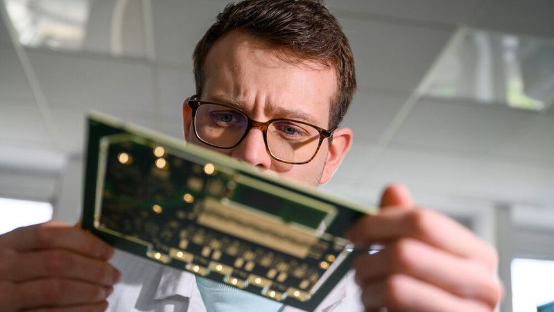
This evolution is particularly noticeable in high-performance electric vehicles, aerospace platforms, maritime systems, motorsport, and non-road mobile machinery (NRMM). In these applications, the move to 800V and beyond battery architectures imposes new constraints in terms of efficiency, electromagnetic compatibility (EMC), transient response, and thermal performance. In these contexts, power conversion becomes more and more a system level engineering problem than just a voltage translation function.
From fixed-ratio conversion to bidirectional power management
Traditional auxiliary converters are typically optimized for a specific voltage ratio and application requirement. However, the increasing fragmentation of electrified platforms has made this design philosophy difficult. High-voltage architectures can be very different from system to system, but the same low-voltage functionality is required for safety-critical electronics and actuation and control systems.
Therefore, modern converter architectures tend to be based on configurability rather than fixed operating points. Promising practical multi-electrification solutions are the wide-input bidirectional topologies for which the HV input can go up to about 1 kV. In addition to voltage transformation, these systems also provide active control of the low voltage bus, such as transient current control and reverse energy flow control.
The transition from unidirectional to bidirectional conversion changes the role of the DC-DC stage radically. The converter is no longer a passive source, but an active player in system stability, able to damp voltage transients and provide peak current without destabilizing sensitive electronics.
:quality(80):fill(efefef,0)/p7i.vogel.de/wcms/6a/02/6a02d06fa2e86/wp-magnachip-sustainably-strong--mastering-the-reduction-of-oxides-coverbild.jpeg "WP_Magnachip_Optimizing 600V SJ MOSFETs for High-Density Server Design_Coverbild")
Why topology still matters more than devices
Although wide-bandgap semiconductors tend to get most of the attention in discussions around next-generation power conversion, selection of topology is still one of the primary determinants of converter performance.
High power HV-LV conversion is increasingly favoring multi-phase interleaved synchronous buck-boost topologies which maintain the efficiency in both step-down and step-up operating modes and allow for smooth changeover of the power flow directions.
The advantage of interleaved architecture is especially important in low voltage, high current operation where conduction losses quickly dominate the switching losses. At the low voltages being delivered at hundreds of amps, switching efficiency is no longer the priority; parasitic resistance, current distribution and thermal management become the design priorities.
By sharing the current between several power stages, the electrical stress on each channel is reduced and the I2R losses are minimized. This method allows high-current operation without excessive thermal penalities when combined with low-resistance switching devices.
Higher switching frequencies usually lead to higher switching losses. But an important trade-off to consider when running near 600 kHz is that passive components can be greatly reduced in size. Lower DC resistance (DCR) of smaller magnetic components helps to offset conduction losses, and also improves thermal dissipation, ultimately allowing for higher power density.
Faster switching, faster control
The shift from silicon MOSFETs to gallium nitride (GaN) transistors is changing the behavior of converters, not just making them more efficient.
One important advantage of GaN devices is the large reduction of parasitic capacitances with respect to the conventional silicon devices. This allows for much higher switching frequencies, rising from the traditional 100-300kHz range to 600 kHz or higher.
The implications are far beyond miniaturizing magnetics. The higher switching speed allows much higher control-loop bandwidths. Digital controllers can react to fast electrical events with high dv/dt and di/dt transitions better.
To provide stability over large conversion ratios, both fast switching and high-bandwidth digital control are needed. Higher frequencies enable control loops to respond more quickly to transient events, improving voltage regulation and allowing smooth transitions between buck and boost operating regions without instability or control saturation.
The resulting improvement in transient response is especially important in actual electrified platforms where loads can change very abruptly and regenerative energy can suddenly come onto the system bus.
:quality(80)/p7i.vogel.de/wcms/b9/26/b9265548cf4e6fe7e45789b711d01f8f/0130098748v2.jpeg "Gallium nitride (GaN) power devices are increasingly challenging silicon MOSFETs in low-voltage power conversion by enabling higher efficiency and switching performance. (Source: AI-generated (OpenAI DALL·E))")
GAN VS. MOSFET
How GaN is killing the MOSFET
Designing for reliability at high dv/dt
The advantages of wide-bandgap switching also bring equally serious engineering challenges. The fast switching transitions increase the dv/dt and di/dt stress levels, making the overall converter reliability more and more dependent on layout optimization, gate-drive integrity, thermal management and parasitic control instead of the semiconductor ratings alone.
The parasitic inductance of PCB plays an important role especially in high frequency GaN system. Improperly controlled switching loops can cause voltage overshoots, ringing and unwanted electromagnetic emissions that can jeopardize reliability and EMC compliance. Thus, the design of the power converter has become an important factor in optimizing electrical performance. Voltage ringing and electromagnetic radiation need to be suppressed by minimizing loop inductance, while preserving switching speed.
Advanced PCB manufacturing techniques (micro-vias, blind vias) enable designers to physically isolate high-power switching loops from low-power control circuitry. Gate-drive paths are isolated from high-current switching nodes to minimize electromagnetic coupling and maintain signal integrity.
The faster the switching event, the more interconnected are electrical, thermal and mechanical design.
Stability beyond the laboratory
The performance of converters is often reported in controlled lab conditions. But real-world electrified systems have other variables that can have a strong effect on behavior.
One of the most important external parameters influencing system stability is the presence of long cable harnesses. The inductance of the cable interacting with fast current transients forms resonant LC networks, which can produce voltage oscillations and ringing. In real installations, bulk decoupling capacitance is needed to damp these resonances and to stabilize voltage rails during fast load changes. Proper cable management and input/output filtering is thus becoming more and more part of the engineering of the converter system, rather than a secondary detail of its implementation.
Fault management is another big challenge. In many applications, immediate shutdown of the converter on overload or short-circuit events may not be the best response, especially in safety-critical systems. High-bandwidth current-limiting loops can be employed to regulate output current at a safe maximum level and maintain converter operation instead. In control theory terms this is like actuator saturation. It limits the output but the system does not stop working and recovers immediately when the fault condition stops.
The engineering behind the next generation of HV-LV conversion
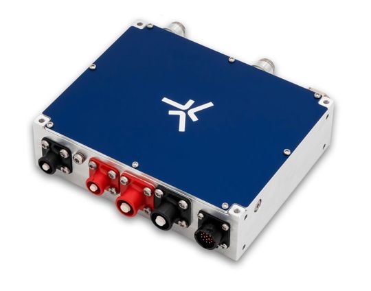
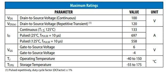
Many of these architectural developments are being fast-tracked through collaborations between semiconductor suppliers and converter specialists. For example, a collaboration between EPC and BrightLoop resulted in the co-engineering of high-power HV-LV conversion platforms using enhancement-mode GaN devices. The work involved device selection, gate driver optimization, switching speed specification, thermal margins and PCB parasitics management for operation at switching frequencies approaching 600 kHz. Evaluation of the devices EPC2302 and validation of next-generation solutions EPC2361 for thermal characteristics and suitability for high-current bidirectional conversion. More generally, this collaboration is indicative of a wider industry trend: successful implementation of wide-bandgap technologies increasingly requires concurrent optimization of semiconductors, control strategies, layout, magnetics, and system-level power architecture, rather than a siloed device substitution approach.
(ID:50855447)
:quality(80)/p7i.vogel.de/wcms/d8/18/d8181873ad07a9b0f77c8ef2d82441cb/0129407783v2.jpeg "Advances in low-voltage GaN devices are enabling higher efficiency and power density in applications traditionally served by silicon MOSFETs. (Source: © roei - stock.adobe.com)")
:quality(80)/p7i.vogel.de/wcms/d6/9a/d69a90a148ae5222d27ac6b33c228a01/0131921521v2.jpeg "A compact three‑phase inverter platform based on the EPC33110 integrated GaN module delivers high switching frequency and power density for robotic joints and lightweight drone propulsion, combining monolithic half‑bridges, integrated drivers and simplified PCB layout. (Source: © Laura - stock.adobe.com)")