SIC MOSFETS Toshiba revolutionizes power conversion with advanced SiC device technology
Related Vendors
Toshiba Electronic Devices & Storage Corporation has developed innovative technology that significantly reduces losses on-resistance1 in silicon carbide trench MOSFETs2 while enhancing UIS ruggedness3. Additionally, Toshiba has developed SiC semi-super junction4 Schottky barrier diodes that suppress the increase in on-resistance at high temperatures. These advances are expected to greatly improve the reliability and efficiency of devices used in power conversion applications, such as electric vehicles and renewable energy systems.
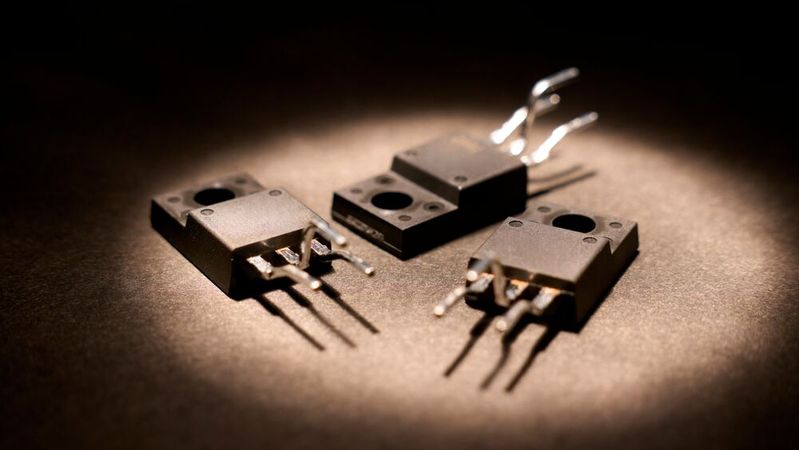
Power semiconductors, which supply and control power, are essential for energy-saving in all electrical equipment, and achieving carbon neutrality. With the electrification of automobiles and the miniaturization of industrial equipment, demand for power semiconductors is expected to continue to grow. This is particularly true of SiC MOSFETs, which are gaining attention as next-generation devices that improve better power conversion efficiency than current silicon (Si)MOSFETs. Among them, SiC trench MOSFETs, where gates are formed in a trench to reduce on-resistance, and SiC Schottky barrier diodes (SBDs), which efficiently convert power by metal semiconductor junction on SiC, are widely used in high-efficiency power conversion applications, such as electric vehicles and renewable energy systems. However, these applications require operation in high-temperature environments that pose challenges for reliability and efficiency improvement.
:quality(80)/p7i.vogel.de/wcms/73/d4/73d402389b7f9d9f0fda92de46b7685f/0113388798.jpeg)
BASIC KNOWLEDGE – SCHOTTKY DIODES
Schottky diode: Definition, applications, and more
SiC trench MOSFETs must protect the gate oxide from high electric fields. However, the relationship between UIS ruggedness and the grounding resistance5 of the electric field protection structure6 has not been clearly understood, making it difficult to achieve both high gate oxide reliability and low on-resistance.
In addition, although SiC SBDs can operate at higher temperatures than conventional Si SBDs, they must be able to handle increased resistance at elevated temperatures, which leads to higher on-resistance.
Toshiba has developed two key technologies to address these issues:
Technology to Improve UIS Ruggedness of SiC Trench MOSFETs
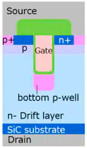
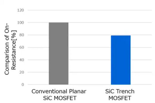
Toshiba has confirmed that forming a protective layer called a Bottom p-well in the trench of SiC trench MOSFETs (Figure 1) and making appropriate reductions in the grounding resistance of the Bottom p-well improves UIS ruggedness. This clarified the previously uncertain relationship between UIS ruggedness and the grounding resistance of the electric field protection structure. The SiC trench MOSFETs prototyped by Toshiba reduced on-resistance by approximately 20 % compared to conventional planar SiC MOSFETs (Figure 2).
Improvement of SiC SJ-SBD Characteristics
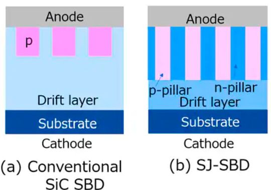
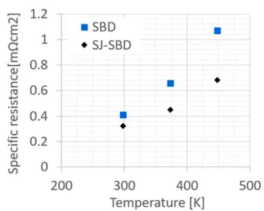
Toshiba also developed SiC SJ-SBDs that reduce resistance in the drift layer by placing pillars7 within in that suppress resistance increases at high temperatures (Figure 3 (b)). By comparing the on-resistance changes in conventional SiC SBDs (Figure 3 (a)) and SiC SJ-SBDs at different temperatures8, Toshiba confirmed the lower on-resistance of the SiC SJ-SBDs, especially at high temperatures (Figure 4). This is due to the SJ structure, which achieves a flat electric field distribution and reduce on-resistance. The 650V SiC SJ-SBDs developed by Toshiba reduces on-resistance by approximately 35 % at high temperatures of 175°C (448.15K) compared to conventional SiC SBDs.
These two technologies further reduce loss in SiC trench MOSFETs and SiC SBDs, improving the reliability and efficiency of devices for use in future high-efficiency power conversion applications. Such application is particularly expected in fields such as electric vehicles and renewable energy systems. Toshiba aims to further improve the technologies and achieve early practical application.
Notes
- 1 On-resistance is the resistance value between the drain and source of a MOSFET during operation (ON)
- 2 MOSFET: Metal Oxide Semiconductor Field Effect Transistor, a switching device with three electrodes: gate, drain, and source. Current between the drain and source is switched on and off by applying a gate voltage.
- 3 UIS (Unclamped Inductive Switching) Ruggedness: A measure of a power device’s ability to withstand energy surges caused by inductive loads during switching. Higher UIS ruggedness indicates better durability and reliability under harsh operating conditions.
- 4 Super Junction (SJ): A structure in which alternating p-type and n-type pillars are formed in the drift layer
- 5 Grounding Resistance: The total resistance of the p-type region extending from the Bottom p-well structure to the source metal.
- 6 Electric Field Protection Structure: A structural feature in trench MOSFETs designed to mitigate the electric field applied to the gate oxide layer when the device is in the off-state (i.e., not conducting current). This helps enhance the reliability of the gate oxide under high-voltage conditions.
- 7 Pillars: Columnar regions of doped semiconductor material formed within the drift layer. In SJ-SBDs, p-type and n-type pillars are alternately arranged to create a super junction structure.
- 8 On-Resistance of SBD: Calculated from the slope of the current–voltage (I–V) curve, with the resistance of the SiC substrate subtracted.
PCIM Expo 2026: Join the leading exhibition!

Lead the future of power electronics! Exhibit your latest solutions, connect with key players, and elevate your brand visibility worldwide at the PCIM Expo from 9 – 11 June 2026 in Nuremberg, Germany. Benefit from our Early Bird discount by 30 June 2025.
Secure your spot now
(ID:50447301)


:quality(80)/p7i.vogel.de/wcms/55/5b/555bb8759d60243792dd736b86585f29/0130909253v2.jpeg)
:quality(80)/p7i.vogel.de/wcms/db/75/db7507346cd4842ca5eb8838f45861ce/0130908924v2.jpeg)
:quality(80)/p7i.vogel.de/wcms/44/0f/440f92984dc6c58eec920824ef55b54c/0130740285v2.jpeg)
:quality(80)/p7i.vogel.de/wcms/be/dc/bedc263ae2b17f59ef71bfc822b95d27/0130740269v2.jpeg)
:quality(80)/p7i.vogel.de/wcms/ea/60/ea600a89db0dc673ba3b6eb1ca56093e/0130736129v2.jpeg)
:quality(80)/p7i.vogel.de/wcms/8b/ae/8bae28ce8ab5e6820bc036ce49939261/0130655531v2.jpeg)
:quality(80)/p7i.vogel.de/wcms/de/9b/de9beb17c1467fdb18301a114f31bf8e/0130651681v2.jpeg)
:quality(80)/p7i.vogel.de/wcms/47/47/474773560a05ff45872e5942c2702e11/0130617850v2.jpeg)
:quality(80)/p7i.vogel.de/wcms/07/89/0789a27b7dcc43dbdafd17f2b601e3a7/0130908474v2.jpeg)
:quality(80)/p7i.vogel.de/wcms/9e/b0/9eb01567f828f28e7922897edc690be2/0130454119v2.jpeg)
:quality(80)/p7i.vogel.de/wcms/db/bb/dbbb1b9c429bd4fc375a7937bb083ba1/0130804041v2.jpeg)
:quality(80)/p7i.vogel.de/wcms/a3/30/a330337e234ac2000bb8829ce34ce001/0130871678v2.jpeg)
:quality(80)/p7i.vogel.de/wcms/34/4a/344a3dc5a19429cf6726b7f8f7e2ee32/0130109719v2.jpeg)
:quality(80)/p7i.vogel.de/wcms/be/c8/bec8d43fc0ee73414274be44608b2970/0129748903v2.jpeg)
:quality(80)/p7i.vogel.de/wcms/23/ee/23ee4a97790d6009dbfd7d9577ffa723/0129220424v2.jpeg)
:quality(80)/p7i.vogel.de/wcms/3c/d1/3cd1cacbceb792ba63727199c61ca434/0127801860v2.jpeg)
:fill(fff,0)/p7i.vogel.de/companies/5f/71/5f71d5f92a5f6/2000px-rogers-corporation-logo-svg.png)
:fill(fff,0)/p7i.vogel.de/companies/66/8b/668becd1c07eb/dowa-logo-word--1-.jpeg)
:quality(80)/p7i.vogel.de/wcms/7d/b4/7db4fc5b8cd18e6eb2c864a3c329f177/0129545524v2.jpeg)
:quality(80)/p7i.vogel.de/wcms/29/99/2999bb9af245dd31f4c837c1d9359046/0128923137v2.jpeg)