SEMICONDUCTOR PACKAGES Resonac unveils high-tech laminates for future semiconductor packages
Related Vendors
Resonac Corporation has developed low thermal expansion copper-clad laminates designated for use in next-generation semiconductor packages that suppress warpage, one of the challenges associated with the increasing size of semiconductor packages.

This product has demonstrated a durability improvement of four times compared to conventional products in temperature cycle testing, making the product suitable for semiconductor packages exceeding 100mm x 100mm. Resonac aims to start mass production of this product in 2026.
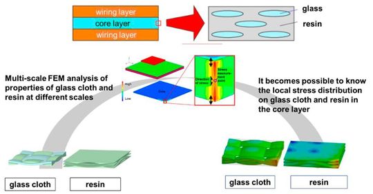
This product was developed by applying “multiscale analysis1,” a computational science technique, to clarify design guidelines for each material that composes the copper-clad laminate. Resonac has incorporated this technology into a general-purpose physical property visualization system, which has now been implemented internally.

In recent years, there has been a trend towards larger package substrates for next-generation semiconductors. However, as the size increases, the impact of substrate warpage on reliability becomes more significant. Typically, to suppress warpage, it is effective to reduce the coefficient of thermal expansion2 of the copper-clad laminate, which is the core material of the substrate. However, this can lead to cracking during the cooling phase of temperature cycle tests due to differences in thermal expansion with other materials that make up the substrate. While design guidelines for reducing cracking (e.g., lowering the modulus of elasticity3) can be suggested, the copper-clad laminate is composed of multiple materials, including resin and inorganic materials (glass cloth), making it difficult to break down those design guidelines into individual material design guidelines.
To address this, Resonac’s Research Center for Computational Science and Informatics applied “multiscale FEM analysis4,” which considers the interaction of physical properties and behaviors between structures of different scales, to the core layer composed of resin and glass cloth in the copper-clad laminate. This approach enabled detailed analysis of localized stress on the resin in the core layer, which is prone to cracking. By controlling specific physical properties of the resin, Resonac developed a copper-clad laminate that reduces generated stress.

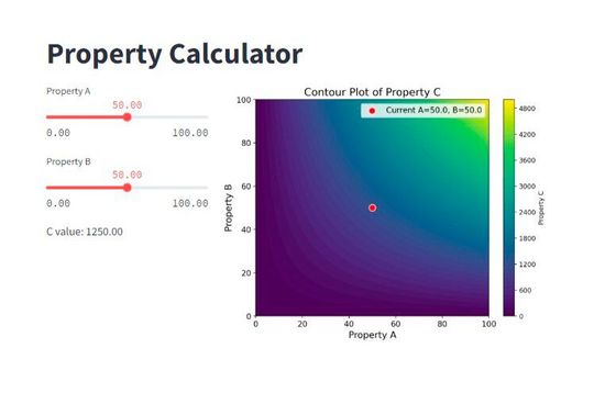
Additionally, Resonac has leveraged this technology to establish a general-purpose physical property visualization system and has begun internal deployment. This system allows users to input the physical properties of materials and visualize how target characteristics (e.g., warpage) change in response. It is applicable not only to copper-clad laminates but also to a wide range of products composed of multiple materials, including molding compounds and film materials. Resonac has started to utilize this system with a focus on products for back-end processes of semiconductor manufacturing, in which Resonac has strength.
With the acceleration of technological innovation in semiconductors, there is an increasing demand for the rapid proposal of high-performance materials. Resonac has allocated 70 % of the resources of its Research Center for Computational Science and Informatics to semiconductor material development, achieving significant results.
Resonac will continue swiftly creating the functionalities demanded by the times, thereby contributing to the sustainable development of the global society.
Notes
- 1 Analysis that couples the physical properties or behaviors of structures at different scales. By homogenizing the material properties of composite materials made from multiple heterogeneous materials, it facilitates understanding of the overall behavior of composite materials.
- 2 Objects expand in volume or length due to a rise in temperature (thermal expansion). The coefficient of thermal expansion indicates how much the volume or length expands with a 1°C rise in temperature, representing a material-specific characteristic.
- 3 A value that indicates the difficulty of deforming a material (the stiffness of the material).
- 4 The Finite Element Method (FEM) divides objects or structures into small elements, quantifying their properties for numerical calculations to analyze the overall behavior, applied to multiscale analysis.
PCIM Expo 2025: Join the industry highlight

Position your company at the forefront of the power electronics industry! Exhibit at the PCIM Expo 2025 in Nuremberg, Germany to showcase your solutions and connect with top decision-makers and innovators driving the industry forward.
Learn more
(ID:50390744)


:quality(80)/p7i.vogel.de/wcms/2f/f3/2ff3221bf7665de2d0acf83760bfd1fa/0130031523v2.jpeg)
:quality(80)/p7i.vogel.de/wcms/c3/16/c316e955a97f5d72d9678297b237b9e5/0129932858v2.jpeg)
:quality(80)/p7i.vogel.de/wcms/ef/0a/ef0adb0acf793fe147cc27c21f6a7a67/0129954238v2.jpeg)
:quality(80)/p7i.vogel.de/wcms/53/f9/53f9301dfc9292d02960f7996c79cc6e/0129927601v2.jpeg)
:quality(80)/p7i.vogel.de/wcms/6e/cd/6ecd41d095d5111cf4ed37b714844487/0129930878v2.jpeg)
:quality(80)/p7i.vogel.de/wcms/02/c0/02c0e9722f70b1134dbf96fb59a9c73d/0129655179v2.jpeg)
:quality(80)/p7i.vogel.de/wcms/cc/67/cc670ea2029cd2af5c641af70e1bf734/0129816392v4.jpeg)
:quality(80)/p7i.vogel.de/wcms/ea/e6/eae6aee30071e67a5627027974437134/0129544613v2.jpeg)
:quality(80)/p7i.vogel.de/wcms/b1/5e/b15ee02b0ba02db70cf61e37d66ad1d3/0129349127v2.jpeg)
:quality(80)/p7i.vogel.de/wcms/26/d5/26d591cc340077026eac56a0e7564faf/0129949603v2.jpeg)
:quality(80)/p7i.vogel.de/wcms/4d/e0/4de02f76a37cbb3df30dd231de589c8e/0128866890v2.jpeg)
:quality(80)/p7i.vogel.de/wcms/18/0b/180b7b63afc91e523592d8a5ce161c96/0129847487v2.jpeg)
:quality(80)/p7i.vogel.de/wcms/be/c8/bec8d43fc0ee73414274be44608b2970/0129748903v2.jpeg)
:quality(80)/p7i.vogel.de/wcms/23/ee/23ee4a97790d6009dbfd7d9577ffa723/0129220424v2.jpeg)
:quality(80)/p7i.vogel.de/wcms/3c/d1/3cd1cacbceb792ba63727199c61ca434/0127801860v2.jpeg)
:quality(80)/p7i.vogel.de/wcms/5a/a0/5aa0436498af618297961fd54ab36cdf/0126290792v2.jpeg)
:fill(fff,0)/p7i.vogel.de/companies/5f/71/5f71d5f92a5f6/2000px-rogers-corporation-logo-svg.png)
:fill(fff,0)/p7i.vogel.de/companies/66/9a/669a2816c84be/pcim-logo.png)
:fill(fff,0)/p7i.vogel.de/companies/66/8b/668becd1c07eb/dowa-logo-word--1-.jpeg)
:quality(80)/p7i.vogel.de/wcms/2a/cc/2accfd11149a6a051be33cb592c3a9f5/0128517332v2.jpeg)
:quality(80)/p7i.vogel.de/wcms/d6/d8/d6d83c11788d14dc3c0b325b477d6137/0128212136v2.jpeg)