POWER EFFICIENCY Quantum dot lasers could redefine power system performance
Related Vendors
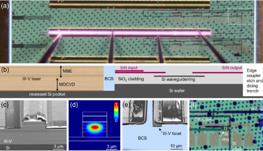
Researchers have demonstrated O-band InAs quantum dot DBR lasers monolithically integrated on silicon photonics using an “in-pocket” heteroepitaxy process, combining two-step epitaxial growth with a polymer gap-fill to achieve low-loss coupling and high thermal stability.

Integrating III–V lasers directly onto silicon photonic platforms has long been a goal for both optical communications and large-scale data infrastructure. Silicon offers manufacturing scalability and CMOS compatibility, but it comes with fundamental drawbacks for light generation: lattice constant mismatches and thermal expansion differences between Si and III–V semiconductors introduce threading and misfit dislocations that degrade optical performance and shorten device lifetime.
While quantum well lasers are highly sensitive to such defects, InAs quantum dot (QD) gain media offer a unique tolerance, maintaining low threshold currents, high temperature stability, and resistance to feedback-induced instabilities even on non-native substrates. The team from the University of California, Santa Barbara, working with collaborators at Aeluma Inc., AIM Photonics, and Analog Photonics, addressed the integration challenge through a “pocket” growth strategy.
In this method, a silicon photonics wafer is etched to create narrow recessed growth pockets, exposing small, defined regions of silicon for localized III–V deposition. These pockets, typically millimeters in length and only 20–50 µm in width, reduce the III–V surface coverage to under 5 % of the wafer while enabling the fabrication of long, narrow ridge waveguide laser sections. By confining the heteroepitaxy to these limited areas, dislocation-related degradation is minimized, and the majority of the wafer remains available for passive photonic circuitry.
:quality(80)/p7i.vogel.de/wcms/84/8c/848c1787435b46a59db45828ed5fffae/0117060285.jpeg)
OPTOELECTRONICS
An introduction to Silicon Photonics
Coupling efficiency and device performance
Historically, one of the most significant barriers to III–V/Si integration has been the coupling loss between the laser output facet and silicon or silicon nitride waveguides. Conventional waveguide-first processes often result in a 5–15 µm air gap between the grown laser and adjacent photonic structures, causing coupling losses above 10 dB.
Techniques like focused ion beam facet polishing can reduce this to about 7.35 dB but are impractical for high-volume production. The UCSB-led team resolved this with a polymer gap-fill approach, creating a low-loss optical bridge between the quantum dot laser facet and the passive waveguide. This process maintains compatibility with ultralow-loss SiN waveguide fabrication, which typically involves high-temperature deposition and annealing steps.

The resulting devices were O-band InAs QD distributed Bragg reflector (DBR) lasers coupled to silicon ring resonators and SiN DBRs. These integrated sources demonstrated single-mode lasing with side-mode suppression ratios up to 32 dB, sustained lasing operation at temperatures as high as 105 °C, and an extrapolated operational lifetime of 6.2 years at 35 °C. Thermal stability is particularly important for densely integrated photonic systems operating in data centers, where elevated ambient temperatures are common. In terms of scalability, the two-step heteroepitaxy process proved essential for maintaining material quality and performance consistency across devices.
Integration potential and the road ahead
By combining pocket heteroepitaxy, two-step epitaxial growth, and polymer gap-fill coupling, the research delivers a monolithic integration pathway that is both high-performance and compatible with silicon photonics foundry processes. This approach allows wafer-scale fabrication of compact, thermally robust laser sources without the packaging complexity of hybrid integration. Importantly, the method avoids disrupting ultralow-loss SiN processing, making it suitable for co-integration with high-performance passive photonic components.
:quality(80):fill(efefef,0)/p7i.vogel.de/wcms/5f/fe/5ffedb2e0ffa6/listing.jpg)
For high-capacity optical interconnects, this technology could lower energy per bit, reduce cooling requirements, and shrink overall system footprints. The compatibility with CMOS-scale wafer processing also opens the door to mass production, supporting applications from hyperscale data centers to advanced telecommunication networks.
While the results are compelling, the pathway to full commercialization still requires targeted refinement. Extending operational lifetimes beyond the current 6.2-year projection, further reducing threshold currents, and confirming high-yield fabrication across full wafer runs will be essential steps. If these advances are achieved, in-pocket InAs QD DBR lasers could transition rapidly from laboratory prototypes to deployed components in next-generation photonic integrated circuits.
For the wider power and communications engineering sectors, this would represent a major leap in integrating energy-efficient, high-bandwidth optical links directly into scalable silicon platforms, driving performance gains without compromising manufacturing efficiency.
PCIM Expo 2026: Join the leading exhibition!

Lead the future of power electronics! Exhibit your latest solutions, connect with key players, and elevate your brand visibility worldwide at the PCIM Expo from 9 – 11 June 2026 in Nuremberg, Germany. Benefit from our Early Bird discount by 30 June 2025.
Secure your spot now
(ID:50516148)


:quality(80)/p7i.vogel.de/wcms/2f/f3/2ff3221bf7665de2d0acf83760bfd1fa/0130031523v2.jpeg)
:quality(80)/p7i.vogel.de/wcms/c3/16/c316e955a97f5d72d9678297b237b9e5/0129932858v2.jpeg)
:quality(80)/p7i.vogel.de/wcms/ef/0a/ef0adb0acf793fe147cc27c21f6a7a67/0129954238v2.jpeg)
:quality(80)/p7i.vogel.de/wcms/53/f9/53f9301dfc9292d02960f7996c79cc6e/0129927601v2.jpeg)
:quality(80)/p7i.vogel.de/wcms/6e/cd/6ecd41d095d5111cf4ed37b714844487/0129930878v2.jpeg)
:quality(80)/p7i.vogel.de/wcms/02/c0/02c0e9722f70b1134dbf96fb59a9c73d/0129655179v2.jpeg)
:quality(80)/p7i.vogel.de/wcms/cc/67/cc670ea2029cd2af5c641af70e1bf734/0129816392v4.jpeg)
:quality(80)/p7i.vogel.de/wcms/ea/e6/eae6aee30071e67a5627027974437134/0129544613v2.jpeg)
:quality(80)/p7i.vogel.de/wcms/b1/5e/b15ee02b0ba02db70cf61e37d66ad1d3/0129349127v2.jpeg)
:quality(80)/p7i.vogel.de/wcms/26/d5/26d591cc340077026eac56a0e7564faf/0129949603v2.jpeg)
:quality(80)/p7i.vogel.de/wcms/4d/e0/4de02f76a37cbb3df30dd231de589c8e/0128866890v2.jpeg)
:quality(80)/p7i.vogel.de/wcms/18/0b/180b7b63afc91e523592d8a5ce161c96/0129847487v2.jpeg)
:quality(80)/p7i.vogel.de/wcms/be/c8/bec8d43fc0ee73414274be44608b2970/0129748903v2.jpeg)
:quality(80)/p7i.vogel.de/wcms/23/ee/23ee4a97790d6009dbfd7d9577ffa723/0129220424v2.jpeg)
:quality(80)/p7i.vogel.de/wcms/3c/d1/3cd1cacbceb792ba63727199c61ca434/0127801860v2.jpeg)
:quality(80)/p7i.vogel.de/wcms/5a/a0/5aa0436498af618297961fd54ab36cdf/0126290792v2.jpeg)
:fill(fff,0)/p7i.vogel.de/companies/60/7e/607ec89d5d9b5/white-frame.jpg)
:fill(fff,0)/p7i.vogel.de/companies/5f/71/5f71d5f92a5f6/2000px-rogers-corporation-logo-svg.png)
:fill(fff,0)/p7i.vogel.de/companies/68/2c/682c3e2e9a195/logotype-rvb.jpeg)
:quality(80)/p7i.vogel.de/wcms/18/0b/180b7b63afc91e523592d8a5ce161c96/0129847487v2.jpeg)
:quality(80)/p7i.vogel.de/wcms/7b/2c/7b2c4ddd6c8fd3b44fe8afc18f0d7e40/0115676667.jpeg)