BASIC KNOWLEDGE Photodiode: Definition, applications, and more
Related Vendors
Photodiodes are important optoelectronic devices that serve various applications like photodetectors, photomultiplier tubes, cameras, and many more. Opposite to LED, photodiodes convert optical energy into electric current. The article explains photodiodes and working principles in detail.
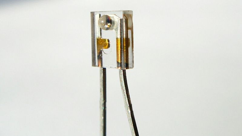
What is a photodiode?
In 1905, Albert Einstein popularly explained the photoelectric effect- the main principle behind photodiodes. The initial photodiode development was related to other related devices such as phototubes and phototransistors. Photodiodes were first developed in the 1960s. Early photodiodes were made from silicon-based PN junctions. The photodiodes made from PIN structure took over the market in the next decade.
Definition photodiode
A photodiode is a two-terminal semiconductor optoelectronic device that absorbs photons to generate current flow in the circuit. The working principle behind photodiode operation is the photoelectric effect. In reverse bias, incident light falls upon the surface of the junction to generate extra charge carriers for current flow. Photodiodes are also called photodetectors, light detectors, and photo sensors.
Photodiode symbol
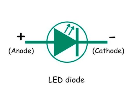
The photodiode symbol depicts two inward rays of incoming photons.
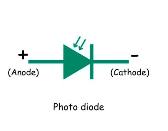
In contrast, the photodiode symbol is the opposite of the LED diode symbol. On the other hand, the LED symbol shows two outward rays of photons.
:quality(80)/p7i.vogel.de/wcms/12/9e/129efd4dca049158c52c34f7f696b6c1/90844911.jpeg)
Renewable Energy
The photoelectric effect and its role in solar photovoltaics
Photodiode working principles
Understanding the fundamental working principles of photodiodes is essential to appreciate how they function as optoelectronic devices, converting incident light into electrical signals efficiently, whether in reverse or zero-bias photovoltaic modes.
Photodiode construction
A photodiode has a PIN structure with an intrinsic layer sandwiched between P-type and N-type semiconductors. The p-layer is diffused over the epitaxial N-substrate. Photodiodes are encapsulated in a casing to prevent physical damage. The casing includes a transparent material to allow wavelengths of light to pass through the device. The intrinsic layer is highly resistive in nature. The addition of an intrinsic layer increases the photodiode’s sensitivity, and response up to frequencies of MHz.
Photodiode working
A photodiode can be called an inverse of an LED. The reason is that photodiodes convert optical input into electric current/voltage but LEDs work opposite to convert electric energy to optical energy. However, both of them are still categorized as optoelectronic devices.
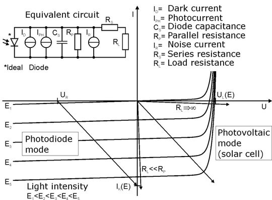
Reverse bias: Photoconducting mode
In reverse bias, current flow due to majority carriers is not possible. It is because of the presence of repulsive force due to the polarity of the voltage. The width of the depletion region widens to prohibit current flow. However, thermally generated minority carriers contribute to a small leakage current flow in the photodiode. The small leakage current, called dark current, flows in the photodiode. The value of dark current is extremely small in the order of nano amperes. It is important to note that dark current flows before the junction is illuminated. Dark current is an unwanted effect of temperature.
:quality(80)/p7i.vogel.de/wcms/d9/64/d964e7b776e5905b69d15374f8b8990b/0115795833.jpeg)
BASIC KNOWLEDGE
The world of power diodes: functions, types, and applications
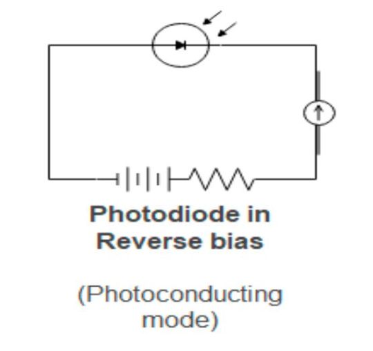
A photodiode operates in a reverse bias mode. The positive terminal of the battery is connected to the N-side and the negative terminal of the battery is connected to the P-side of the photodiode. The photoconducting mode enables current flow in the photodiode. When the depletion region is exposed to light in reverse bias, the photodiode starts to multiply the charge carriers to initiate drift current flow.
Imagine a light ray incident on the surface of the photodiode. The incident light falling on the junction of a photodiode can excite the electrons. The frequency of incident photons must be greater than the threshold frequency of the material.
The circuit diagram of the photodiode in reverse bias is represented along with a constant voltage source and a resistance.
The work function of a material is defined as the minimum amount of energy required to excite and transfer a bonded electron from a lower energy valence band to a higher energy conduction band. The work function of incident light should be higher than the work function of the material. In simple words, incident photons transfer the energy to the electrons to initiate current flow in the photodiode.
A scintillation crystal casts light on the junction of the photodiode. The phenomenon where incident light with a higher frequency than the threshold frequency knocks off electrons from a material’s surface is called the photoelectric effect. The ejected electrons are termed as photoelectrons. The photoelectric effect is the main working principle behind photodiodes.
:quality(80)/p7i.vogel.de/wcms/ff/22/ff22163c256104c22639a24e8af3565b/0113258006.jpeg)
TYPES OF DIODES - OVERVIEW
The different diode types explained
In the given diagram below, E1 is the lower energy level valence band and E2 is the higher energy level conduction band. Before incident light falls on the surface of the photodiode, electrons reside in the stable lower energy balance band E1. Let us imagine an incoming photon with a higher work function compared to the junction material, hitting the surface of the photodiode.
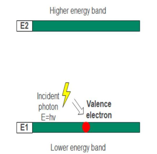
The process in which the energy from an incident photon is absorbed to excite an electron from low energy to a higher energy level is called absorption. The electron reaches a higher E2 energy level from the lower E1 energy level. The electron leaves a hole behind in the valence band. The hole functions as a positive charge in semiconductors.
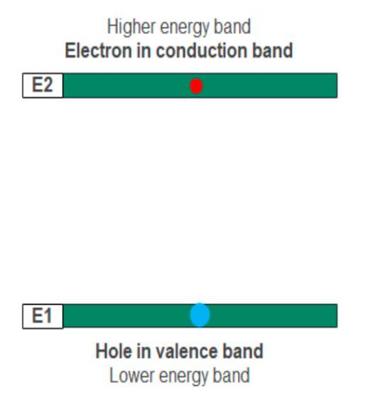
The generation of electron-hole pairs causes drift current flow in the photodiode. The current flow due to incident light is called photocurrent or light current. The value of photocurrent is in the order of microamperes. Simply put, a photodiode utilizes radiation as an external energy source to generate extra carriers in the junction. These extra carriers flow through the circuit and generate electric current output.
Zero bias: Photovoltaic mode
In photovoltaic mode, there is no biasing voltage or extremely low bias. When the depletion region is exposed to the light, photons generate electron-hole pairs. The zero bias or low bias restricts photocurrent flow out of the circuit. The diagram below represents a photodiode with zero biasing voltage.
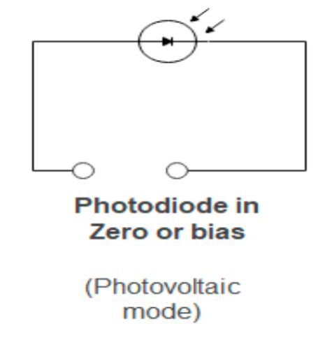
Whether the photodiode circuit is open or has a load impedance, a voltage develops between the two terminals. The built-in electric field generates a potential difference in which the anode is positive with respect to the cathode. Simply put, the potential difference generates a forward voltage in the order of millivolts to volts. Now this photocurrent is called forward current.
The application of photovoltaic mode is to generate electric power from the incident light without the application of a biasing voltage or at extremely low bias. The selection of load impedance is crucial to get desirable voltage output and optimal power extraction.
:quality(80):fill(efefef,0)/p7i.vogel.de/wcms/5f/fe/5ffedb2e0ffa6/listing.jpg)
Forward bias (Not important/less used)
In forward bias, photodiodes do not respond to incident light. Electrons get thermally excited to reach higher energy bands. An undesirable dark current flows through the photodiode as a function of temperature. Forward dark current contributes to noise, signal degradation, heating, and battery drainage. In simple words, a photodiode behaves like a normal diode in forward bias.
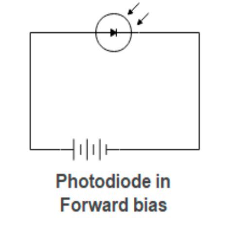
It is better to use a normal PN junction or PIN diode instead of the photodiode in forward bias to save the project's costs. In practice, photodiodes are manufactured only to operate in either reverse or no bias. Photodiode data sheets do not mention the magnitude of forward current because it holds no significance in electronics.
Photodiode characteristics
The photodiode characteristic curve shows the constant value of photocurrent upon application of increasing reverse bias voltage.
Photodiode types
PN Photodiode: A photodiode was initially a simple PN junction diode. PIN-structured photodiodes were later developed to offer better results in applications.
PIN Photodiode: The current photodiodes in the market have a PIN structure. PIN structures make photodiodes more sensitive and responsive.
APD (Avalanche Photodiode): The avalanche photodiodes utilize impact ionization and avalanche effect to generate more photocurrent. Similar to photodiodes, avalanche diodes operate in reverse bias. The collision of atoms generates more electron-hole pairs. In addition to the photoelectric effect, the secondary emission multiplies charge carriers to allow heavy current flow. The drawback associated with avalanche photodiodes is high noise.
Photodiode applications
Photodiodes are essential components in various optical and electronic systems, where they play a crucial role in detecting and converting light into electrical signals.
- Photodetectors, photosensors, smoke detectors, photoconductors, and photomultiplier tubes.
- Imaging devices.
- Computed tomography.
- Electric isolation in optocoupler.
- Cameras and TVs.
- Solar panels and photovoltaic cells.
- Optical fibers.
- Electric power generation from incident light.
:quality(80)/p7i.vogel.de/wcms/f5/d5/f5d5285ddfc4d02f5279413129bbad71/0114199240.jpeg)
BASIC KNOWLEDGE - DIODES
All about diodes - One direction, many paths
Photodiode advantages
The advantages of photodiodes make them valuable components in various optical and electronic applications, offering reliable and versatile performance.
- Compact.
- Low cost.
- High sensitivity to infrared, UV, visible light, gamma, and X-rays.
- Good linear and spectral response.
- Low-voltage operation.
- Small dark current.
Photodiode disadvantages
Despite their multiple advantages, photodiodes have certain limitations that need to be considered in specific applications.
- Prone to failure.
- Less temperature stability.
- Limited range.
- Small active region.
- Noise due to dark current.
How to test a photodiode?
The long terminal of the photodiode is the anode (positive) and the slightly shorter terminal is the cathode (negative).
- Take a multimeter and set it to “Diode function”.
- Connect the negative probe (black) to the COM or common terminal of the multimeter.
- Connect the positive probe (red) to the Voltage option.
- Connect the positive probe to the anode and the negative probe to the cathode of the photodiode.
- The reading mentions “1”. Displaying such a low reading indicates that the photodiode blocks dark current.
- Bring a light source near the diode.
- The multimeter reading goes on to increase to indicate photocurrent flow.
- Repeat the same procedure to find multimeter readings for reverse bias connection.
- Connect the positive probe to the cathode and the negative probe to the anode of the photodiode.
- Bring a light source near the photodiode to notice changes in the readings.
(ID:49995496)


:quality(80)/p7i.vogel.de/wcms/55/5b/555bb8759d60243792dd736b86585f29/0130909253v2.jpeg)
:quality(80)/p7i.vogel.de/wcms/db/75/db7507346cd4842ca5eb8838f45861ce/0130908924v2.jpeg)
:quality(80)/p7i.vogel.de/wcms/44/0f/440f92984dc6c58eec920824ef55b54c/0130740285v2.jpeg)
:quality(80)/p7i.vogel.de/wcms/be/dc/bedc263ae2b17f59ef71bfc822b95d27/0130740269v2.jpeg)
:quality(80)/p7i.vogel.de/wcms/ea/60/ea600a89db0dc673ba3b6eb1ca56093e/0130736129v2.jpeg)
:quality(80)/p7i.vogel.de/wcms/8b/ae/8bae28ce8ab5e6820bc036ce49939261/0130655531v2.jpeg)
:quality(80)/p7i.vogel.de/wcms/de/9b/de9beb17c1467fdb18301a114f31bf8e/0130651681v2.jpeg)
:quality(80)/p7i.vogel.de/wcms/47/47/474773560a05ff45872e5942c2702e11/0130617850v2.jpeg)
:quality(80)/p7i.vogel.de/wcms/07/89/0789a27b7dcc43dbdafd17f2b601e3a7/0130908474v2.jpeg)
:quality(80)/p7i.vogel.de/wcms/9e/b0/9eb01567f828f28e7922897edc690be2/0130454119v2.jpeg)
:quality(80)/p7i.vogel.de/wcms/db/bb/dbbb1b9c429bd4fc375a7937bb083ba1/0130804041v2.jpeg)
:quality(80)/p7i.vogel.de/wcms/a3/30/a330337e234ac2000bb8829ce34ce001/0130871678v2.jpeg)
:quality(80)/p7i.vogel.de/wcms/34/4a/344a3dc5a19429cf6726b7f8f7e2ee32/0130109719v2.jpeg)
:quality(80)/p7i.vogel.de/wcms/be/c8/bec8d43fc0ee73414274be44608b2970/0129748903v2.jpeg)
:quality(80)/p7i.vogel.de/wcms/23/ee/23ee4a97790d6009dbfd7d9577ffa723/0129220424v2.jpeg)
:quality(80)/p7i.vogel.de/wcms/3c/d1/3cd1cacbceb792ba63727199c61ca434/0127801860v2.jpeg)
:fill(fff,0)/p7i.vogel.de/companies/63/c7/63c7da97be945/diotec.png)
:fill(fff,0)/p7i.vogel.de/companies/5f/71/5f71d5f92a5f6/2000px-rogers-corporation-logo-svg.png)
:fill(fff,0)/p7i.vogel.de/companies/66/8b/668becd1c07eb/dowa-logo-word--1-.jpeg)
:quality(80)/p7i.vogel.de/wcms/18/0b/180b7b63afc91e523592d8a5ce161c96/0129847487v2.jpeg)
:quality(80)/p7i.vogel.de/wcms/7b/2c/7b2c4ddd6c8fd3b44fe8afc18f0d7e40/0115676667.jpeg)