BASIC KNOWLEDGE - DIODES All about diodes - One direction, many paths
Related Vendors
The diode is one of the oldest semiconductor devices that date back to the late nineteenth century. Before solid-state semiconducting diodes, vacuum diodes held the utmost significance. This article explains the diode and its working, applications, and testing in detail. It lists types of diodes and tries to give you an idea about them in brief.

1. What is a diode
Diodes started as “valves”- the devices that allow unidirectional current flow but slowly evolved into semiconductors for half a century. 24-year-old German physicist Ferdinand Braun proposed the idea of semiconductor diodes. The inventor of the cathode ray tube (CRT) studied the behavior of crystals extensively at Würzburg University to present the idea of a solid-state diode in 1876.
Another British scientist John Ambrose Fleming patented the thermionic diode in 1904 and 1905 in Britain and US respectively. Years passed by and valve diodes were holding a significant portion of the market. The domination of semiconductor diodes and transistor technologies in the 1960s paved the way for modern semiconducting diodes.
Diode Definition
A diode is a two-terminal extrinsic semiconductor device that conducts electric current in a single direction. The unidirectional current flow of the diode made it to be called a “valve” historically. It is because diodes allow current flow in one direction and block current in the other simultaneously. However, this current is bipolar due to majority and minority charge carrier movement.
2. Diode symbol - the key to electronic functionality
The symbol of a diode is an iconic one in the world of electronics. It represents the basic function and properties of this versatile component. The diode symbol consists of a triangle connected to a horizontal line. The triangle shows the arrow in the direction of current flow, while the horizontal line represents the separation between the anode and cathode.
This simple but meaningful symbol is key to electronic functionality. It shows that diodes allow current to flow in a certain direction while blocking current flow in the opposite direction. This property makes diodes indispensable for a wide range of applications, from rectifying current to signal modulation and light emission.

3. What does a diode do?
A diode allows current flow in one direction through a low-resistance path and blocks the flow in another direction with high resistance. It is similar to the historically popular “one-way valve” that allowed unidirectional current flow.
4. How does a diode work?
An ideal diode is a hypothetical device that does not exist in reality. Usually, the ideal diode is capable of performing a “perfect” operation for the applications. Practically existing diodes try to follow ideal diode characteristics with some deviations and exceptions. Depending upon the biasing voltage or voltage polarities, the ideal diode can operate within the conducting and non-conducting regions.
An ideal diode is said to be in forward bias when the positive terminal of the battery is connected to the anode and the negative terminal of the battery is connected to the cathode. The forward bias arrangement makes the ideal diode behave like a short-circuit (closed switch) with zero resistance.
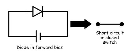
As RID = 0
The voltage across the diode is VID = 0
According to Ohm's law
VID = IID * RID
0 = IID = 0/0
IID = ∞
The ideal diode in forward bias is said to be a perfect conductor. The direction of the conventional current flow is from positive to negative or anode to cathode.
An ideal diode is said to be in reverse bias when the negative terminal of the battery is connected to the anode and the positive terminal of the battery is connected to the cathode. The reverse bias arrangement makes the diode behave like an open circuit that allows zero current flow during the operation.
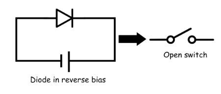
As IID = 0
The voltage across the diode is VID = 0
According to Ohm's law
VID = IID * RID
0 = 0 * RID
RID = 0/0
RID = ∞
The ideal diode in reverse bias is said to be a perfect insulator. The direction of the conventional current flow is from negative to positive or cathode to anode.
Characteristics of an ideal diode
The V-I characteristics of a diode are the graph of voltage on the X-axis and current on the Y-axis to understand the conducting behavior of the diode. An ideal diode is a type of electronic device whose conducting state and characteristics depend upon the type of biasing voltage. The characteristic curve of an ideal diode resembles a switch, which can be either logically ON or OFF.
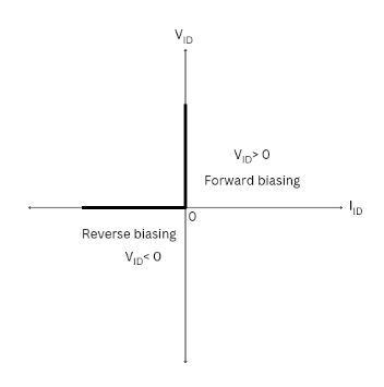
However, a diode cannot possess infinite current or resistance practically. The ideal behavior of the diode is limited by the circuit and various practical conditions like doping quality, minority charge carriers, barrier potential, etc.
Practical diode
A practical diode or simply a diode is the physical device that is the closest version of the ideal diode. It is an extrinsic semiconductor that tries to follow the characteristics and perform similar functions to that of the ideal diode. However, a practical diode does not obey Ohm’s law and shows non-linear V-I characteristics.
Using doping techniques like diffusion or deposition, a trivalent impurity forming a P-type material is applied on a wafer containing a pentavalent impurity forming the N-region. The physical boundary that divides both types of semiconducting materials is known as the junction.
A diode has two terminals: cathode (K) or N-side and anode (A) or P-side. An external voltage, called a bias, is applied to the diode for enabling current conduction.
Electrons are the majority charge carriers in the N-region but minority charge carriers in the P-region. Similarly, holes are majority charge carriers in the P-region and minority charge carriers in the N-region.
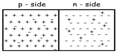
Electrons in the N-side diffuse into the P-side and holes in the P-side diffuse into the N-side.
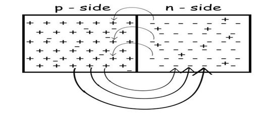
The diffusion of charge carriers results in the formation of an insulating layer inside the diode.
Diode under no bias
The diffusion of electrons gathers negative ions- acceptor ions on the P-side. Holes in the P-side diffuse into the N-side to gather positive ions- donor ions in the N-region. In simple words, the majority of charge carriers from both sides cross the junction which leads to the formation of negative ions on the P-side and positive ions on the N-side. The region that contains positive or negative ions but is devoid of any mobile charge carriers (electrons or holes) is known as the depletion layer or space charge region. The average thickness of a depletion region lies between 10-4 to 10-7 meters.
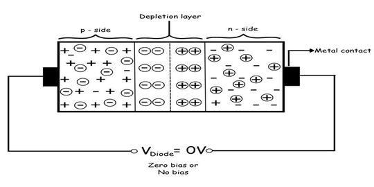
In the depletion region, an electric field is generated from positive ions to the negative ions, i.e. from N-side to P-side. While the conventional current flow is from the P side to the N side. The electric field opposes the diffusion tendency of holes and electrons by applying force in the opposite direction to their movement.
The lowest voltage at which the opposing electric field exists in the junction is known as barrier potential. When a diode is given sufficient input voltage, it exceeds the barrier potential and allows the current to flow. The charge carriers must possess kinetic (or thermal) energy to cross the depletion layer against the electrostatic force of attraction or repulsion and start current flow in the device.
The minimum voltage at which charge carriers gain enough energy to cross the junction and the depletion region vanishes in a diode is known as cut-in voltage or knee voltage. In simple words, it is defined as the minimum voltage called threshold voltage, denoted by VT, that allows current to flow inside a diode. Since the diode is a semiconductor device, the cut-in voltage is 0.7 V for Silicon and 0.3 V for Germanium materials respectively.
Forward bias: Diode “ON”
A diode is said to be in the forward bias when the P-side is connected to the positive terminal and N-side is connected to the negative terminal of the battery.
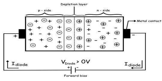
The connection enables electrons on the N-side and holes on the P-side to gain sufficient kinetic energy due to the attractive forces generated by battery polarity. Electrons and holes combine with the ions near their regions respectively and reduce the width of the depletion layer.
The remaining 90-95 % of electrons and holes cause heavy currents to flow due to attractive forces and reduced depletion layer length. The current increases exponentially and the width of the depletion layer reduces with increased input forward voltage. The attractive forces at the ends support the current flow only in one direction. Hence, the diode turns on upon application of a forward voltage greater than the threshold voltage.
Reverse bias: Diode "OFF"
A diode is said to be in the reverse bias when the P-side is connected to the negative terminal and N-side is connected to the positive terminal of the battery.
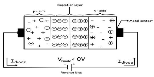
The reverse connection disables the electrons in the N-side and holes in the P-side to cross the junction due to the increasing width of the depletion layer. A large number of electrons move towards the positive potential and holes move towards the negative terminal. The repulsive movement causes an increase in the number of positive and negative ions in the N and P regions which increases the width of the depletion layer.
However, a very small current, known as reverse current, flows through the minority carrier electrons on the P-side and holes on the N-side. The reverse current soon reaches a saturation value and does not increase beyond low microamperes for high input reverse voltage. Hence, the diode remains off in reverse bias.
Diode current flow
| Diode Biasing | Direction of current flow |
| Forward Bias | P to N Anode to Cathode |
| Reverse Bias | N to P Cathode to Anode |
Diode models
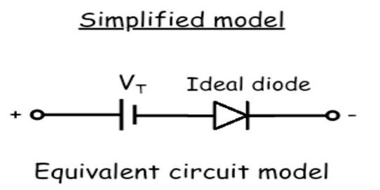
There are various models for understanding the operation of diodes. Such models combine an ideal diode, a battery, and a resistor. Corresponding characteristics of the models are studied for understanding the operational behavior. Some of those popular models include piecewise-linear and simplified.
The simplified model of a diode shows a diode connected to a battery representing the threshold voltage.
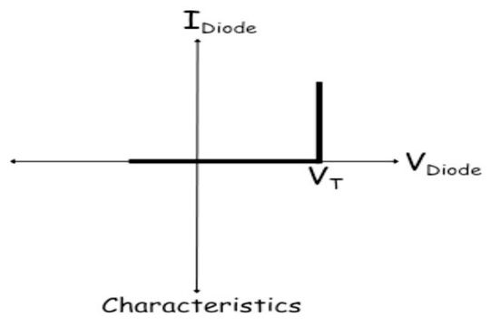
The VI characteristics of the simplified model are different from the practical diode.
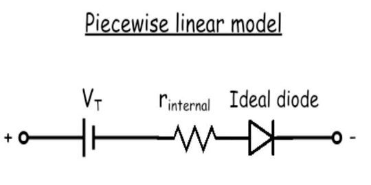
In the piecewise-linear model, an ideal diode is connected to a battery representing threshold voltage and a resistor that combines the internal resistances of P and N-type semiconductor materials. The resistance is known as bulk resistance or internal resistance, denoted by RB or Rinternal.
The VI characteristics of the piecewise-linear model are somewhat similar to the practical diode.
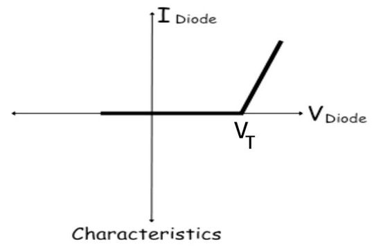
However, there are more regions of operation in a practical diode.
V-I characteristics of a practical diode
Just like an ideal diode, the VI characteristics of a practical diode show the relationship between voltage and current in forward and reverse bias regions. The conducting state of the diode starts in forward bias operation. As soon as the input voltage crosses the threshold voltage, the diode starts conducting.
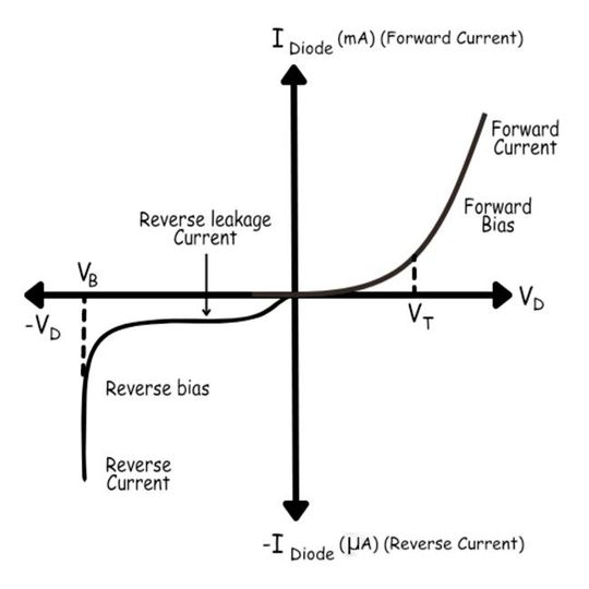
The reverse bias diode shows that a very small leakage current flows in the device initially. With the constant increase in reverse voltage, the current suddenly increases exponentially. The phenomenon of the sudden increase in current during the reverse bias of the diode is called breakdown. The maximum reverse voltage at which breakdown occurs in a diode is called peak inverse voltage. It is also the maximum voltage a diode can withstand without breakdown (or damage). Electrical breakdown is the state where an insulating material enters the state of electrical conduction. It is because the minority charge carriers knock off bonded electrons and cause the current flow. The voltage at which electrical breakdown occurs is known as the breakdown voltage of the diode.
Diode current equation
The graph of Ohm’s law states that the relationship between current and voltage should be linear. Practically, semiconductor diodes show a non-linear voltage and current relationship. The diode current equation or Shockley diode equation is a medium that helps electronics engineers to understand and calculate the values of current flowing in the diode as a function of the biasing voltage.
IDiode = IO (eVDiode/ƞVT -1)
As VT = KT/q, the diode-current equation becomes
IDiode = I0 (eVDiode q/ƞkT - 1)
Where
- VDiode is the diode voltage in Volts
- VT is the threshold voltage in Volts (Si = 0.7 V, Ge = 0.3 V)
- IDiode is the current flowing in the diode, expressed in A (Ampere) or mA (Milliampere).
- IO is the temperature-dependent saturation current in μA (Microampere).
- T is the absolute junction temperature in K (Kelvin).
- k is Boltzmann’s constant 1.38 x 10⁻²³ J/K
- q is the charge of electrons or holes with polarity 1.6 x 10⁻¹⁹ Coulombs
- η is the ideal out factor (Si = 2, Ge = 1)
5. Types of diodes
There are numerous types of diodes developed for different applications and requirements. Each diode type has specific properties and characteristics that make it suitable for certain tasks. But what are the main differences between diode types? In this section, the most important diodes - such as Zener diodes, Schottky diodes and many others are listed and briefly explained.
Zener diode
A Zener diode is similar to a PN junction diode but is heavily doped instead. The diode works on the “Zener effect” and is operated in reverse bias as a voltage regulator, clipper circuits, or shift registers.
Schottky diode
A Schottky diode is a type of diode where a metal is bonded to an N-type semiconductor. The threshold voltage is lesser than 0.7 V of a Silicon diode. Schottky diodes are used in TTL and CMOS logic families.
LED diode
A light-emitting diode (LED) works on the principle of electroluminescence, in which an electrical source of energy produces light (photons). Since electron-hole recombination means reaching a lower-energy state, the energy released is heat or light.
Laser diode
A laser diode is similar to an LED diode but uses an external voltage source. Electric current supports the recombination of electrons and holes to release photons. Such diodes are used extensively in fiber optics, bar codes, and laser printers.
Double diode
Historically, electronic vacuum tubes were popular before semiconductor devices. A double diode is not exactly a diode but a vacuum tube, used in American radio receivers. Also known as a “double diode triode”, the device had a single triode and two electrodes, then referred to as diodes.
Power diode
A Power diode is a high-power PN junction diode with an additional lightly doped N- drift layer. It has three layers- a heavily doped P+ region, a lightly doped N- drift layer, and a heavily-doped N+ layer.
Flyback diode
A Flyback diode (flywheel or snubber diode) is used with an inductor to reduce the voltage spike due to the sudden removal of supply. The diode allows the current to take an alternate path, performing a similar function to snubber circuits.
Photodiode
A Photodiode works on the principle of the “photoelectric effect”- the production of electric current upon consumption of light energy. Intense photons strike a PN or PIN diode that knocks off electron-hole pairs and produces a current known as photocurrent.
Super barrier diode
A Super Barrier Rectifier is a proprietary device from Diodes Incorporated. The MOS manufacturing process allows the diode to obtain low forward voltage and thermal stability. SBR is used in buck/boost converters, solar panels, and LEDs.
Rectifier diode
Usually, all diodes perform the function of rectification- conversion of alternating current to direct current. However, the Rectifier diode is specially used in bridge rectifiers in a combination of four or six.
Small Signal diode
The word “small signal” signifies an AC signal, making these diodes applicable in waveform clipping, and clamping. The small signal diodes have a smaller junction area to reduce the junction capacitance, making them perform well in higher frequencies.
P-N junction diode
The PN junction is the most basic type of diode, a foundation of all diodes. PN junction diode combines N and P-type semiconductors, where the diode conducts in forward bias.
Gunn diode
A Gunn diode is constructed by using three n-type semiconductor layers. A lightly-doped N-type layer is embedded between two heavily doped N+ layers. The doping profile makes the device exhibit negative résistance characteristics, suitable for microwave and radio astronomy.
PIN diode
The PIN diode stands for P-type — Intrinsic — N-type semiconductor. A narrow intrinsic semiconductor (undoped), mostly Silicon, is introduced between the heavily doped P and N-type materials to allow for maximum reverse voltage.
Tunnel diode
A tunnel diode is a heavily doped PN junction diode that operates on the principle of “quantum tunneling”. The heavy doping reduces the width of the depletion region enough to support the quantum tunneling of electrons.
Varactor diode
A Varactor diode or Varicap provides electrically controllable capacitance. During reverse bias, the depletion layer thickness increases but capacitance decreases. The varactor diode is manufactured to provide variation of capacitance with a low input reverse voltage.
Vacuum diode or Thermionic diode
A vacuum diode or thermionic diode is not exactly a semiconductor diode but a device that allows a unidirectional flow of current. It is more like a vacuum tube with two electrodes that allow current flow from the cathode to the anode and block the other direction.
Transition voltage suppression diode (TVS)
A Transition voltage suppression diode (TVS) is a type of avalanche diode that operates in reverse bias. The diode is used to clamp overvoltages for a shorter time, making it a suitable protection for electronics.
Shockley diode
A Shockley diode was one of the first semiconductor devices invented to be used in computers and telecommunications. However, the Shockley diode was not actually a diode but a four-layer PNPN semiconductor similar to a Thyristor.
Stabistors or forward reference diode
A Stabistor is a simple Silicon diode that offers a stable VI characteristic in forward bias operation. The device is used for the regulation of lower voltages and offers stable values for a wide range of currents.
Gold-doped diode
A gold-doped diode is a silicon diode with an introduction of gold dopant using solid-state diffusion techniques. The gold diffusion reduces leakage current and controls recombination density, affecting the reverse recovery time, minority carrier lifetime, and charge storage capabilities.
Snap-off or Step recovery diode
A step recovery diode (SRD) works on the principle of preventing electron-hole recombination through the generation of high minority charge carriers. SRDs are used in microwave frequencies to generate short pulses.
Thermal diode
A Thermal diode is a device used in thermal management systems to perform the function of thermal rectification. The device blocks the flow of heat to the system and adjusts the voltage in a device as a function of temperature.
Crystal diode
Crystal diodes were used before PN junction diodes in microwave applications. Also known by the name of cat’s whisker or point contact diodes, these devices work on the magnitude of contact between pressed metal wire and materials such as lead sulfide.
Avalanche diode
An Avalanche diode is just like a Zener diode due to reverse bias operation but is lightly doped, causing the breakdown to occur at higher voltages. Avalanche diodes are used in SPAD receivers for digital signal processing.
Constant current diode
A constant current diode acts like a diode but is an n-channel JFET with a gate shorted to the source terminal. It is a two-terminal device with a cathode and anode that limit current to a specified value.
Quantum well diode
A Quantum well laser diode is a type of diode where the active region of the diode is made thin enough to support quantum confinement. It is similar to that of Laser diodes but works on the principle of “quantum wells”.
6. Diode applications
Diodes are not just simple electronic components; they are the relentless workhorses of the electronics world, fulfilling a myriad of crucial functions in virtually every electronic device. But what does a diode do? This fundamental question paves the way for our exploration into the vast applications of diodes. From converting alternating current to direct current, shaping electrical signals, to protecting sensitive circuits – diodes are omnipresent wherever electronics are involved.
Here is a list of the most common applications of diodes:
- Rectification: As diodes allow only unidirectional current flow, they perform the function of rectification- converting alternating current to direct current. The bridge rectifier is one of the most popular rectifiers used in systems.
- Signal shaping: Diodes shape electrical signals in clipping and clamping circuits. Clipper circuits truncate waveforms and clampers shift the waveform to a fixed level.
- Switching: The unidirectional flow of current makes diodes applicable as short circuits and open switches.
- Digital Logic: Diodes are a building block of logic gate realization in digital electronics. Diode-Resistor Logic (DRL) and Diode-Transistor Logic (DTL) families were popular before the development of the latest technologies.
- Protective circuits: Diodes are part of protective circuits in electronic devices. For example, diodes protect a system from overvoltage by stabilizing the voltage. Zener diodes are one of the most suitable options for voltage regulation.
- Power electronics: Diodes perform rectification for power supplies, improve system efficiency in power correction circuits, and are used as voltage multipliers. Flyback diodes (similar to snubber circuits) are effectively used for voltage spikes.
- RF and Microwave: Diodes such as Gunn diodes are extensively used in Microwave. Other functions of diodes in microwaves include frequency multiplication, microwave filters, limiters, modulation, and many more applications.
- Optics: Photodiodes, LED diodes, and laser diodes are applicable in optics. Other applications include optical communication, optical isolation, and optical sensing.
- Communication system: Diodes are used in demodulation techniques such as AM and FM in communication systems.
- Renewables: Diodes are used in energy storage systems by modification of minority carrier lifetime. In wind turbines, diodes control the current flow. Another major application of diodes is in solar energy systems, solar cells, and photovoltaics.
7. How to test a diode
A diode can be easily tested using a digital multimeter because of a direct button. However, the direct button may not always be present.
Diode test analysis
Step 1: Set the rotary switch to the “Diode” icon on the multimeter.
Step 2: Forward bias the diode by touching the red lead on the anode (P-side) and black lead on the cathode (N-side). The forward voltage drop is always nearer to the value of the threshold voltage.
Step 3: Reverse bias the diode by touching the black lead on the anode (P-side) and red lead on the cathode (N-side). The multimeter should display 0L when the diode is reversed-biased.
A damaged open diode shows 0L for the same values in both directions.
Watch this video to get explained how to test a diode:
Resistance mode test
Step 1: Set the rotary switch to “Resistance Mode” on the multimeter.
Step 2: Forward bias the diode by touching the red lead on the anode (P-side) and black lead on the cathode (N-side). The value of resistance ranges from 100 ohms to 1 mega ohms for a functional diode.
Step 3: Reverse bias the diode by touching the black lead on the anode (P-side) and red lead on the cathode (N-side). The value of resistance must be 0L for a functional or undamaged diode.
A damaged diode produces the same values in both directions.
References
Boylestad, R., & Nashelesky, L. (2012). Electronic Devices and Circuits Theory (11th ed.). Pearson Education.
Sharma, S.K., & Jerath, R. (2014). New Millennium Physics. S. Dinesh & Co.
(ID:49706141)


:quality(80)/p7i.vogel.de/wcms/55/5b/555bb8759d60243792dd736b86585f29/0130909253v2.jpeg)
:quality(80)/p7i.vogel.de/wcms/db/75/db7507346cd4842ca5eb8838f45861ce/0130908924v2.jpeg)
:quality(80)/p7i.vogel.de/wcms/44/0f/440f92984dc6c58eec920824ef55b54c/0130740285v2.jpeg)
:quality(80)/p7i.vogel.de/wcms/be/dc/bedc263ae2b17f59ef71bfc822b95d27/0130740269v2.jpeg)
:quality(80)/p7i.vogel.de/wcms/ea/60/ea600a89db0dc673ba3b6eb1ca56093e/0130736129v2.jpeg)
:quality(80)/p7i.vogel.de/wcms/8b/ae/8bae28ce8ab5e6820bc036ce49939261/0130655531v2.jpeg)
:quality(80)/p7i.vogel.de/wcms/de/9b/de9beb17c1467fdb18301a114f31bf8e/0130651681v2.jpeg)
:quality(80)/p7i.vogel.de/wcms/47/47/474773560a05ff45872e5942c2702e11/0130617850v2.jpeg)
:quality(80)/p7i.vogel.de/wcms/07/89/0789a27b7dcc43dbdafd17f2b601e3a7/0130908474v2.jpeg)
:quality(80)/p7i.vogel.de/wcms/9e/b0/9eb01567f828f28e7922897edc690be2/0130454119v2.jpeg)
:quality(80)/p7i.vogel.de/wcms/db/bb/dbbb1b9c429bd4fc375a7937bb083ba1/0130804041v2.jpeg)
:quality(80)/p7i.vogel.de/wcms/a3/30/a330337e234ac2000bb8829ce34ce001/0130871678v2.jpeg)
:quality(80)/p7i.vogel.de/wcms/34/4a/344a3dc5a19429cf6726b7f8f7e2ee32/0130109719v2.jpeg)
:quality(80)/p7i.vogel.de/wcms/be/c8/bec8d43fc0ee73414274be44608b2970/0129748903v2.jpeg)
:quality(80)/p7i.vogel.de/wcms/23/ee/23ee4a97790d6009dbfd7d9577ffa723/0129220424v2.jpeg)
:quality(80)/p7i.vogel.de/wcms/3c/d1/3cd1cacbceb792ba63727199c61ca434/0127801860v2.jpeg)
:fill(fff,0)/p7i.vogel.de/companies/63/c7/63c7da97be945/diotec.png)
:fill(fff,0)/p7i.vogel.de/companies/5f/71/5f71d5f92a5f6/2000px-rogers-corporation-logo-svg.png)
:fill(fff,0)/p7i.vogel.de/companies/61/dc/61dc0e8c2e420/dspace-logo-1000px-220107.png)
:quality(80)/p7i.vogel.de/wcms/d9/64/d964e7b776e5905b69d15374f8b8990b/0115795833.jpeg)
:quality(80)/p7i.vogel.de/wcms/35/f2/35f243dd4bd4d57587bd7e4f7a85d6fa/0117752002v2.jpeg)