ELECTRONIC WASTE A new greener substrate to tackle e-waste
Related Vendors
Growing consumption demand, IoT, and the release of new portable electronic devices drive the e-waste crisis. The semiconductor fabrication process generates a significant amount of e-waste. Researchers at MIT, the University of Utah and Meta have developed a flexible substrate material for multilayer semiconductor fabrication. The article talks about a new substrate material that can combat e-waste.

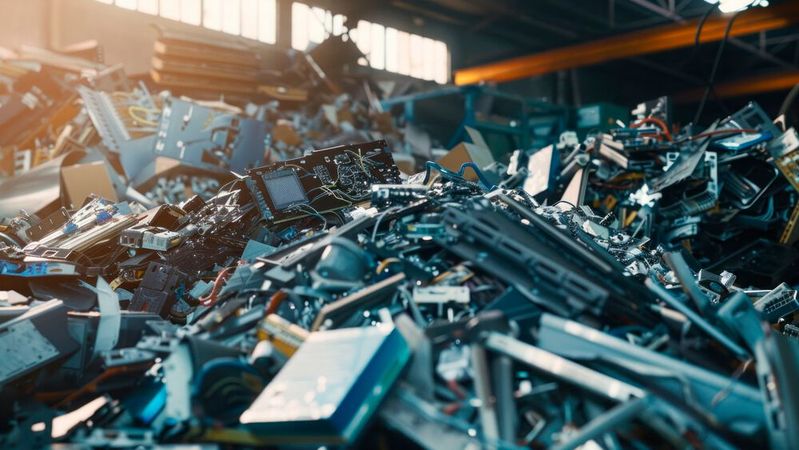
Electronic waste or e-waste comprises a wide range of discarded or used electronic devices, components, circuit boards, wires, etc. Such electronic devices and components are thrown away after years of use or at replacement time. Globally, e-waste is a major environmental issue because it contaminates soil, air and water with harmful chemical releases. International regulatory bodies have defined standards to manage, process, and recycle e-waste.
The processes involved in manufacturing the end product generate tonnes of e-waste. Historically, factories would throw this waste into water bodies. However, many countries have banned such practices. The year 2022 marked 62 million tonnes of e-waste. The amount is estimated to reach 82 million tonnes by 2030. The newly generated waste is accumulated with undisposed or unrecycled waste, making the situation even more critical.
E-waste from semiconductor fabrication
Fabrication units implement traditional methods to manufacture the substrate material for semiconductors. The traditional methods generate a significant amount of unwanted heat.
In addition, electronics manufacturing involves the use of expensive materials such as copper, nickel, and sometimes even silver and gold. As a result, recycling and reprocessing e-waste is an economical benefit for hardware manufacturers.
Several chip manufacturers have emerged as climate-change advocates with their R&D department focusing on creating reusable components.
:quality(80):fill(efefef,0)/p7i.vogel.de/wcms/5f/fe/5ffedb2e0ffa6/listing.jpg)
MIT discovers a new substrate material
The researchers at MIT, the University of Utah and Meta have successfully created a new re-processable material for semiconductor substrates. The following section details the experiment and demonstrates potential benefits.
Problem with green materials
Unreliable devices: There are many problems associated with the use of green materials in semiconductor substrates. Historically, using green materials to build semiconductor substrates compromises the mechanical, thermal, and dielectric capabilities of the end-stage product. As a result, a greener substrate material tends to produce unreliable semiconductor devices.
Heat wastage: Polyamide (PI) is a polymer used to build greener substrates with exceptional mechanical, thermal, and dielectric properties. However, the internal PI bonds are strong enough to break at higher temperatures. High-temperature reprocessing wastes heat and deteriorates the ability to build a miniaturized circuit again.
Synthesizing polymers
Custom diallyl bisimide monomers were synthesized at high temperatures. The results confirmed that all the polymers were thermally, mechanically, and chemically stable with low dielectric losses. The experiment produced a flexible and optically clear thin film, which can be used in commercial-grade substrates to build a functional semiconductor circuit.
The new invention vs. legacy
Researchers compared the film to the legacy industrial aromatic polyimide film called “Kapton”. Kapton has been used for years in industries such as PCB, 3D printing, aerospace, automotive, and medical equipment manufacturing. But Kapton is limited to a one-time use, impractical to reprocess.
The experiment compared thin-film to Kapton in terms of thermal, mechanical, chemical, and dielectric properties. The polyamides showed better thermal conductivity with comparable thermal stability and dielectric losses to Kapton. Beyond comparable properties, the research explored depolymerization.
Depolymerization
If polymerization helps to build substrate, depolymerization enables extracting back meaningful elements from the material. Simply put, depolymerization recovers electric components from polymers for reuse.
Kapton cannot be depolymerised. The experiment used methanol and potassium carbonate to depolymerise the thin film. The entire process took a week. A revised method added 50 % dichloromethane to finish the entire process in 24 hours.
Real-world integration
The experiment was taken further to test a real-world circuit. Basic electronic components with simple routing circuits were added to the 100-micrometer thick film made from PI-ester resin. Shadow mask and PVD (Physical Vapor Deposition) created a thin circuit pattern.
The film was dipped into a liquid metal Eutectic gallium indium alloys (EGaIn) solution. Basic components like LED, resistor, and coin battery were assembled properly for the test. The assembled circuit was fully functional. Values of resistances, voltages, and current were noted for reference.
:quality(80)/p7i.vogel.de/wcms/ba/ef/baef3496e4ee9bf88468e08206e8e7e8/88323983.jpeg)
IoT
How to get power supply for IoT devices right
Results
The fully functional circuit was immersed in a solution of 50 % dichloromethane, 50 % methanol and 0.07 M potassium carbonate at room temperature. Within two hours, the PI-ester substrate was depolymerised. The same components were rinsed and tested again for functionality. Surprisingly, the values of the resistor and LED matched the previous ones.
Summarizing the experiment
Custom diallyl bisimide monomers were synthesized and used in thiol-ene photopolymerization to produce reprocessable polymer networks. The resulting polymer showcased exceptional and comparable properties to commercial aromatic polyimide Kapton in electronic substrate applications. The depolymerization processes involved selective removal of the substrate to recover fully functional electronic components. The experiment involved UV rays to process the new material. The room-temperature depolymerization process and recovery of fully functional components confirmed that the new development is reprocessable.
A step forward
Researchers have developed degradable photopolymerizable polyimide to build smooth-surface substrates that do not require high-temperature processing. The entire process can recover used electronic components like resistors and LEDs.
Researchers suggest creating multilayered circuits through the photopolymerization of selected areas and the removal of unnecessary resin. The new redistribution layer enables the proper current flow with the necessary insulation.
The internal chemistry of these polymers is compatible with modern fabrication workflows. The solution is effective and economically feasible. The University of Utah team has co-founded a new company to improve and commercialize greener technology to combat e-waste.
(ID:50133756)


:quality(80)/p7i.vogel.de/wcms/55/5b/555bb8759d60243792dd736b86585f29/0130909253v2.jpeg)
:quality(80)/p7i.vogel.de/wcms/db/75/db7507346cd4842ca5eb8838f45861ce/0130908924v2.jpeg)
:quality(80)/p7i.vogel.de/wcms/44/0f/440f92984dc6c58eec920824ef55b54c/0130740285v2.jpeg)
:quality(80)/p7i.vogel.de/wcms/be/dc/bedc263ae2b17f59ef71bfc822b95d27/0130740269v2.jpeg)
:quality(80)/p7i.vogel.de/wcms/ea/60/ea600a89db0dc673ba3b6eb1ca56093e/0130736129v2.jpeg)
:quality(80)/p7i.vogel.de/wcms/8b/ae/8bae28ce8ab5e6820bc036ce49939261/0130655531v2.jpeg)
:quality(80)/p7i.vogel.de/wcms/de/9b/de9beb17c1467fdb18301a114f31bf8e/0130651681v2.jpeg)
:quality(80)/p7i.vogel.de/wcms/47/47/474773560a05ff45872e5942c2702e11/0130617850v2.jpeg)
:quality(80)/p7i.vogel.de/wcms/d8/20/d820f7b4d986659548161686fb97209c/0130929474v2.jpeg)
:quality(80)/p7i.vogel.de/wcms/ef/1c/ef1c6a123496f3c00da6ea8b85385de9/0130926273v2.jpeg)
:quality(80)/p7i.vogel.de/wcms/07/89/0789a27b7dcc43dbdafd17f2b601e3a7/0130908474v2.jpeg)
:quality(80)/p7i.vogel.de/wcms/9e/b0/9eb01567f828f28e7922897edc690be2/0130454119v2.jpeg)
:quality(80)/p7i.vogel.de/wcms/34/4a/344a3dc5a19429cf6726b7f8f7e2ee32/0130109719v2.jpeg)
:quality(80)/p7i.vogel.de/wcms/be/c8/bec8d43fc0ee73414274be44608b2970/0129748903v2.jpeg)
:quality(80)/p7i.vogel.de/wcms/23/ee/23ee4a97790d6009dbfd7d9577ffa723/0129220424v2.jpeg)
:quality(80)/p7i.vogel.de/wcms/3c/d1/3cd1cacbceb792ba63727199c61ca434/0127801860v2.jpeg)
:fill(fff,0)/p7i.vogel.de/companies/62/b9/62b980cddf5d6/ceramtec.png)
:fill(fff,0)/p7i.vogel.de/companies/68/ba/68baa33f71e37/logo-pcim.png)
:fill(fff,0)/p7i.vogel.de/companies/5f/71/5f71d5f92a5f6/2000px-rogers-corporation-logo-svg.png)
:quality(80)/p7i.vogel.de/wcms/f0/d8/f0d82f06ed1b7abb3245dfc4c317cb55/0127949994v2.jpeg)
:quality(80)/p7i.vogel.de/wcms/b1/0a/b10a283cdf3e5f156781a7273c71a7e0/0129107484v2.jpeg)