


:quality(80)/p7i.vogel.de/wcms/7f/4b/7f4b97757cea82c0675209630577dc22/0133974130v2.jpeg "Vox Power’s EIRE600 delivers up to 600 W in a compact 5 × 3-inch package, with forced-air or conduction cooling options for industrial and medical equipment. (Source: Vox Power)")
:quality(80)/p7i.vogel.de/wcms/55/97/5597c3436e3bc92ee7ba23b6f9d289e9/0134032539v2.jpeg "Littelfuse’s TP7.0SMD-XC automotive TVS diode series uses foldback technology to provide low clamping voltage for protecting sensitive vehicle electronics. (Bild: Littelfuse)")
:quality(80)/p7i.vogel.de/wcms/51/f8/51f84448e666230bb11a02566abd1177/0133958187v3.jpeg "Microchip’s radiation-tolerant GaN point-of-load converter supplies up to 20 A for space-based processors, FPGAs, microcontrollers and ASICs. (Source: Microchip)")
:quality(80)/p7i.vogel.de/wcms/0a/7c/0a7c08f368ae1d91f758dd18d2a32e88/0133978423v2.jpeg "EPFL researchers have demonstrated a GaN transistor that withstands nearly 4 kV, using an intrinsic polarization superjunction design to distribute electric fields more evenly. (Source: EPFL)")
:quality(80)/p7i.vogel.de/wcms/5b/94/5b94232ca4183d6fcc2dccc7394d7544/0134041114v4.jpeg "Siemens and NVIDIA are testing AI applications at Siemens’ Erlangen electronics factory, using digital twins to support production planning and prepare inspection systems before physical prototypes are available. (Bild: Siemens)")
:quality(80)/p7i.vogel.de/wcms/b4/1f/b41f2731a07b608e60eca3663e280301/0133980549v2.jpeg "Multi-year agreement with Wolfspeed supports Infineon’s conversion from 150-millimeter to 200-millimeter silicon carbide (SiC) manufacturing (Source: © Ada - stock.adobe.com)")
:quality(80)/p7i.vogel.de/wcms/e3/0a/e30a8813bcf44b16f0dceb63a0747d29/0133984094v2.jpeg "The semiconductor is only one part of the design. Higher voltage, frequency and power density also increase the demands on electronic packaging materials such as die attach, substrates, top-side interconnects and module attach. (Source: Generated by AI)")
:quality(80)/p7i.vogel.de/wcms/5d/fb/5dfba5e5f38daf2b8597b05656af29c0/0133956337v2.jpeg "Wolfspeed has received a conditional commitment for a loan of up to $1.5 billion from the U.S. Department of War to support its domestic wide-bandgap semiconductor supply chain. (Source: © AspctStyle - stock.adobe.com)")
:quality(80)/p7i.vogel.de/wcms/bf/b6/bfb6ac295759be32d567df9849b6767e/0134094495v2.jpeg "Fraunhofer ISE reports that 25 Ah pouch cells with silicon-rich anodes retained more than 83% of their initial capacity after 1,000 cycles when tested under 1,000 kPa axial pressure. (Bild: Fraunhofer ISE)")
:quality(80)/p7i.vogel.de/wcms/16/dc/16dca55e6ef80e6b5da68bc628da2dcc/0133844782v2.jpeg "This article explains virtual power plants in modern renewable-heavy grids. (Source: © M@rketVisualsStudio - stock.adobe.com)")
:quality(80)/p7i.vogel.de/wcms/e8/33/e8330aae4bea3578b98ec2c1403d367a/0133980001v2.jpeg "IRENA’s 2026 World Energy Transition Outlook identifies faster electrification powered by renewables as central to meeting future global energy needs. (Source: Irena)")
:quality(80)/p7i.vogel.de/wcms/6c/b4/6cb405f47d25035e256ae90fe3a66ee6/0134032112v2.jpeg "Sungrow’s PowerTitan 3.0 energy storage platform uses onsemi EliteSiC hybrid power modules, with the companies reporting peak inverter efficiency above 99.3%. (Bild: onsemi)")
:quality(80)/p7i.vogel.de/wcms/7b/76/7b76005554b556df2a7a3794bdf69d44/0132365246v2.jpeg "Hioki’s ST5680A DC Hipot Tester combines CE/UKCA/CSA compliance, an integrated capacitance‑based contact check and time‑series waveform recording (voltage, leakage current, insulation resistance) to standardize hipot and insulation testing across EV cell, module and pack production lines. (Source: Hioki)")
:quality(80)/p7i.vogel.de/wcms/af/7f/af7f7b0fb7f29219fc991b1130f65477/0132241333v2.jpeg "Comprehensive laboratory testing regimens—combining thermal cycling, high‑current stress, EMC, and accelerated lifetime tests—are essential to validate advanced power designs and ensure reliability in real‑world applications. (Source: PRBX)")
:quality(80)/p7i.vogel.de/wcms/16/3d/163df69363f8125315a9826e13ea4b05/0131927425v2.jpeg "Solution will maximize data center and AI factory profitability while delivering engineering-grade insights to design and operations for more efficient, sustainable, and resilient infrastructure. (Source: Cadence)")
:quality(80)/p7i.vogel.de/wcms/85/b7/85b7e90733a2bd8f21515d8f7137f2fc/0131917677v2.jpeg "Renesas acquires Pictorus to integrate its embedded application software platform with Renesas’ MCU and MPU portfolio, helping developers shorten time‑to‑market and simplify system integration. (Source: © lucadp - stock.adobe.com)")
:quality(80)/p7i.vogel.de/wcms/f8/34/f834240d434a0c265a2ccafe614c8cd7/0134032109v4.jpeg "Hard- and soft-switching techniques shape voltage and current during device transitions, influencing switching losses, EMI and thermal performance in power converters. (Bild: © Mrthullab - stock.adobe.com)")
:quality(80)/p7i.vogel.de/wcms/27/07/2707280c807689b437baed3660257404/0133626052v2.jpeg "The quantum behavior of electrons shapes semiconductor devices—and the power converters that deliver electricity to modern computing systems. (Source: © Celt Studio - stock.adobe.com)")
GAN DEVICES Infineon ships new 40V CoolGaN BDS devices
Related Vendors
:fill(fff,0)/p7i.vogel.de/companies/62/a0/62a0a0de7d56a/aic-europe-logo.jpeg "aic-europe-logo (AIC Europe)")
:fill(fff,0)/p7i.vogel.de/companies/5f/71/5f71d5f92a5f6/2000px-rogers-corporation-logo-svg.png "2000px-Rogers_Corporation_Logo.svg.png (rogers germany)")
Infineon Technologies AG expands its CoolGaN BDS 40 V G3 bidirectional switch (BDS) family with two new devices, the IGK048B041S and IGK120B041S. The new additions reduce PCB footprint by up to 82 percent and cut component count in half. For engineers designing within the strict spatial constraints of modern smartphones, notebooks, and wearables, this is a significant and quantifiable step forward.
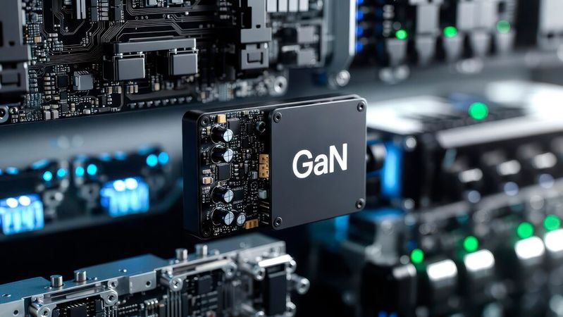
Targeting compact consumer devices, the new devices give power system designers greater flexibility to optimize efficiency and streamline designs without sacrificing performance.
“As consumer devices continue to shrink while power demands grow, engineers face increasing pressure to deliver more from less. The new CoolGaN BDS devices directly address this challenge,” said Johannes Schoiswohl, GaN Business Line Head at Infineon. “Each device integrates the function of two back-to-back silicon MOSFETs into a single component, reducing component count by half and simplifying PCB layouts. Design teams can leverage existing driver layout, avoiding costly redesigns and accelerating time to market. The result is a leaner and more cost-effective power path.”
The BDS, like other GaN devices, is compatible with 5 V gate drive. Offered in WLCSP chip-scale packages measuring 2.1 x 2.1 mm2 and 1.7 x 1.2 mm2, the IGK048B041S and IGK120B041S are engineered for the tight spatial constraints of smartphones, notebooks and wearables. The larger GaN device achieves 4.2 mΩ RDD(on) while the smaller device delivers 9 mΩ RDD(on). The CoolGaN BDS devices further distinguish themselves through superior switching and leakage performance. Gate charge is up to approximately 40% lower than comparable competing devices. Lower gate charge translates directly to faster switching transitions, reduced switching losses, and improved system efficiency in fast-charging applications. Additionally, Drain-Drain Leakage current is more than 85% lower than competing solutions, underscoring the inherent leakage advantages of GaN technology. Together, these characteristics reduce thermal rise, supporting long-term reliability and helping manufacturers meet increasingly stringent safety requirements.
Unlike silicon MOSFETs, which rely on a body diode that can allow unintended current flow, the CoolGaN BDS devices allow bidirectional voltage and current blocking. This true bidirectional blocking capability is essential for applications such as USB overvoltage protection in smartphones and portable devices, where preventing unwanted reverse current is critical to protecting sensitive downstream components. The devices are equally well-suited to load switching and power multiplexing functions in multi-rail power architectures, where precise control of current direction across multiple supply rails is required.
With the addition of these two devices, the Infineon CoolGaN BDS 40 V G3 family now comprises three devices – the IGK048B041S, IGK120B041S, and the previously released IGK080B041S – addressing the full spectrum of mobile power switching requirements from compact wearables to high-performance notebooks.
Infineon has a strong portfolio with more than 40 new GaN product announcements in the last year and is a preferred partner for customers seeking high-quality GaN solutions. The company is on track with its implementation of scalable GaN manufacturing on 300-millimeter wafers with first samples already being shipped to customers. 300 mm GaN enables higher production capacity and faster delivery of high-quality GaN products, which further strengthens Infineon’s position in the GaN market.
(ID:50859243)
:quality(80)/p7i.vogel.de/wcms/5c/70/5c702b0346478ec842bb253ab10824ec/0127931956v4.jpeg "Symbolic Image: Infineon’s CoolGaN powers Enphase’s next-gen IQ9 solar microinverters. (Source: © ABCDstock - stock.adobe.com)")
:quality(80)/p7i.vogel.de/wcms/da/f4/daf432573fac7d099d1b9fad5196c3f9/0130217438v2.jpeg "Renesas introduces a 650 V bidirectional GaN switch designed to improve efficiency and enable new architectures in power conversion systems for solar, energy storage, and AI data centers. (Source: Renesas)")