BASIC KNOWLEDGE How to draw and calculate a MOSFET amplifier circuit
Related Vendors
This article details the main calculations required for the design of a simple single-stage MOSFET amplifier. It reveals key parameters such as transconductance, drain current, and voltage gain, considering the amplifier's operation in its active region and applying basic circuit analysis concepts. Without considering thermal aspects that influence the calculations or attempting to address the circuit implementation for building an application, the example offers an interesting introduction to the operation of an enhancement-mode MOSFET amplifier.

MOSFETs are commonly used in power electronics as small-signal linear amplifiers due to their high input impedance, which facilitates biasing, and their fast switching speed, which makes them ideal for high frequencies. They also consume little current and are very efficient, offering good thermal stability and linear performance.
The most notable applications are found in power electronics devices, such as power supplies and converters, as well as in high-fidelity audio systems and for switching in mobile devices and processors. Its ability to amplify audio and radio frequency (RF) signals and to manage energy effectively is remarkable.

Among the industries that use MOSFET amplifiers are automotive, where they are found in electric vehicles and control electronics; consumer electronics, found in phones, tablets, and game consoles; medical devices; and audio and telecommunications, where they are used as part of high-fidelity and RF amplifiers.
As an effective option for voltage amplification, enhancement-mode MOSFETs are used in a common-source configuration, and are the most widely used type of FET amplifier in integrated circuits due to their ability to generate very low noise levels.
Enhancement N-channel MOSFET amplifier
eMOSFET amplifier uses a metal-oxide silicon transistor connected in the common source configuration.

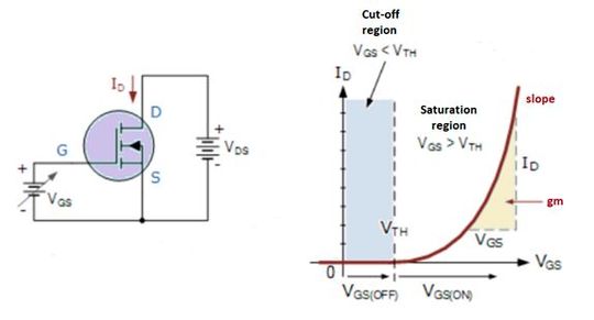
To obtain the graph of the MOSFET's forward DC characteristics, we can plot the drain current, ID, values with varying values of VGS by connecting a fixed drain-source voltage VDS to the eMOSFET.
These characteristics give the transconductance, gm which relates the output current to the input voltage and represents the gain of the transistor.
gm = ΔID/ΔVGS
This ratio is measured in units of Siemens (S), or amperes per volt.
In the MOSFET, the conductivity of the channel region is enhanced by the field effect as we gradually increase the positive gate-source voltage VGS. The point where the channel begins to conduct is called the threshold voltage VTH.
When the eMOS transistor is operating in the saturation or conducting region the drain current, ID is given by:
ID = k(VGS - VTH)2
where k is the conduction parameter.
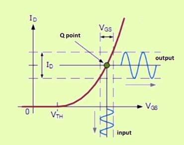
The MOSFET's quiescent point Q is defined by establishing the desired drain current, for which it is biased within the saturation region. This point must be located approximately halfway between the supply voltage VDD and the threshold voltage VTH, thereby achieving maximum output voltage swing.
DC bias point = (VDD – VTH)/2

Basic MOSFET Amplifier

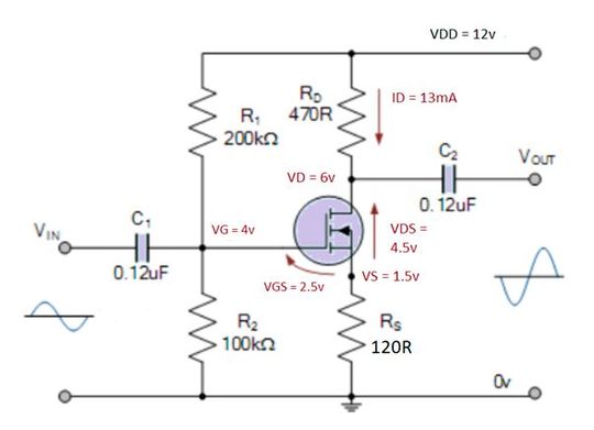
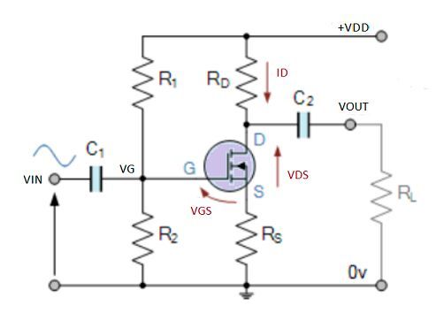
This simple enhancement-mode common source MOSFET amplifier configuration uses a single supply at the drain and generates the required gate voltage, VG using a resistor divider.
VDD = IDRD + VDS + IDRS
= ID(RD + RS) + VDS
RD + RS = (VDD - VDS)/ID
Then from this we can say that:
RD = (VDD - VD)/ID and RS = VS/ID
and the MOSFET gate-to-source voltage, VGS is given as:
VGS = VG - ISRS
The gate-source voltage must be greater than the MOSFET's threshold voltage (VGS > VTH) for the MOSFET to function properly. Since IS = ID, the gate voltage, VG is therefore equal to:
VGS = VG - IDRS
VG = VGS + IDRS
or V<G = VGS + VS
As a rule, the drain terminal DC bias voltage is set to half the supply voltage, ensuring a symmetrical, distortion-free output waveform.
VD = VDD/2
The gate voltage of the MOSFET amplifier is calculated by selecting the appropriate values for the bias resistors R1 and R2 within the voltage divider network. With no current flowing into the gate terminal of a MOSFET device, the formula for voltage division is given as:
VG = VDDR2/(R1 + R2)
To reduce the power loss across the resistors (I2R) and increase the input impedance RIN of the MOSFET amplifiers, the values of these two resistors are set as large as possible.
RIN = R1R2/(R1 + R2)
If we set the lower cutoff frequency for the MOSFET amplifier to 20 Hz,
f(-3 dB) = 20 Hz = 1/2π RIN C
Then, input and output coupling capacitors (C1,C2), C = 1/2π f RIN
:quality(80):fill(efefef,0)/p7i.vogel.de/wcms/5f/fe/5ffedb2e0ffa6/listing.jpg)
Considerations to keep in mind
Among the most common mistakes when designing a MOSFET amplifier are failure to bias the Q-point (quiescent point) and not to consider the effect of temperature when selecting components, leading to circuit oscillation, overheating, or poor performance.
The first cause can be due to the Q-point being located in the cutoff or saturation regions, poor polarization stability under temperature variations, or improperly sized resistors in the bias circuit. It manifests itself as a distorted output signal or with insufficient or no amplification.
A solid understanding of device behavior in its operating region, combined with a mastery of key concepts such as biasing and linearity, ensure successful design and calculation of a basic enhancement-mode MOSFET amplifier. Starting with a detailed analysis of key electrical parameters using the device's characteristic operating curve, this article proposes step-by-step calculations of voltage levels, resistance values, and gain, analyzing the circuit in a simple common-source configuration.
The purpose of this study is not to address a real-life application, as additional aspects affecting calculation accuracy, such as temperature effects and component tolerances, are not taken into account. However, they serve as a starting point for simulation or prototyping stages in many basic amplifier designs in power electronics.
(ID:50531869)


:quality(80)/p7i.vogel.de/wcms/2f/f3/2ff3221bf7665de2d0acf83760bfd1fa/0130031523v2.jpeg)
:quality(80)/p7i.vogel.de/wcms/c3/16/c316e955a97f5d72d9678297b237b9e5/0129932858v2.jpeg)
:quality(80)/p7i.vogel.de/wcms/ef/0a/ef0adb0acf793fe147cc27c21f6a7a67/0129954238v2.jpeg)
:quality(80)/p7i.vogel.de/wcms/53/f9/53f9301dfc9292d02960f7996c79cc6e/0129927601v2.jpeg)
:quality(80)/p7i.vogel.de/wcms/6e/cd/6ecd41d095d5111cf4ed37b714844487/0129930878v2.jpeg)
:quality(80)/p7i.vogel.de/wcms/02/c0/02c0e9722f70b1134dbf96fb59a9c73d/0129655179v2.jpeg)
:quality(80)/p7i.vogel.de/wcms/cc/67/cc670ea2029cd2af5c641af70e1bf734/0129816392v4.jpeg)
:quality(80)/p7i.vogel.de/wcms/ea/e6/eae6aee30071e67a5627027974437134/0129544613v2.jpeg)
:quality(80)/p7i.vogel.de/wcms/b1/5e/b15ee02b0ba02db70cf61e37d66ad1d3/0129349127v2.jpeg)
:quality(80)/p7i.vogel.de/wcms/26/d5/26d591cc340077026eac56a0e7564faf/0129949603v2.jpeg)
:quality(80)/p7i.vogel.de/wcms/4d/e0/4de02f76a37cbb3df30dd231de589c8e/0128866890v2.jpeg)
:quality(80)/p7i.vogel.de/wcms/18/0b/180b7b63afc91e523592d8a5ce161c96/0129847487v2.jpeg)
:quality(80)/p7i.vogel.de/wcms/be/c8/bec8d43fc0ee73414274be44608b2970/0129748903v2.jpeg)
:quality(80)/p7i.vogel.de/wcms/23/ee/23ee4a97790d6009dbfd7d9577ffa723/0129220424v2.jpeg)
:quality(80)/p7i.vogel.de/wcms/3c/d1/3cd1cacbceb792ba63727199c61ca434/0127801860v2.jpeg)
:quality(80)/p7i.vogel.de/wcms/5a/a0/5aa0436498af618297961fd54ab36cdf/0126290792v2.jpeg)
:fill(fff,0)/p7i.vogel.de/companies/63/c7/63c7da97be945/diotec.png)
:fill(fff,0)/p7i.vogel.de/companies/5f/71/5f71d5f92a5f6/2000px-rogers-corporation-logo-svg.png)
:fill(fff,0)/p7i.vogel.de/companies/69/30/693022b11e5db/logo.jpeg)
:quality(80)/p7i.vogel.de/wcms/2c/26/2c26bbdc79651af5c70c0971c2aa25ba/0125756269v2.jpeg)
:quality(80)/p7i.vogel.de/wcms/b9/18/b918d8d0e447a18f7b9e983c25b96330/0125855402v2.jpeg)