GaN vs. MOSFET Evaluating GaN as a low-voltage alternative to Silicon MOSFETs
Related Vendors
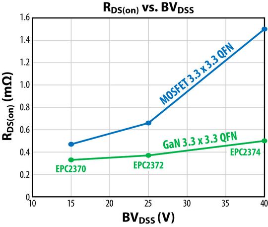
Recent advancements in gallium nitride (GaN) power devices demonstrate a substantial expansion of their operational range into low-voltage applications under 40 V. Silicon MOSFETs have historically dominated this voltage range due to their good conduction performance, well-understood manufacturing processes, and proven reliability.

Improvements introduced in seventh-generation GaN devices now enable performance levels that make GaN technically viable in applications previously considered unsuitable. These developments are particularly relevant in systems where high current density, fast transient response, and limited thermal headroom dominate design constraints.
The power MOSFET market is large and well-established, and is expected to reach around $14 billion by 2027. It is generally divided into three voltage segments: below 40 V, 40–200 V, and above 600 V, with the segment below 200 V accounting for roughly 75% of the total market. This is the segment where low-voltage GaN devices have the greatest impact, including applications such as AI servers, 48 V power converters, robotics, and autonomous machines.
By offering higher efficiency, increased power density, and simplified system design, seventh-generation GaN technology is increasingly positioning itself as a viable alternative to silicon in modern low-voltage power conversion systems.
:quality(80)/p7i.vogel.de/wcms/8d/e0/8de08e7cf8c954f00d30a4a1894a8294/0126807438v2.jpeg)
COMPARISON
Battle of SiC vs GaN power modules
Device-level improvements enabling low-voltage operation
In the past, GaN generations worked better at higher voltages, where switching losses were the biggest problem and the wide-bandgap material properties could be fully used. But at lower voltages, conduction losses become more important, and the benefits of GaN were canceled out by higher effective on-resistance and parasitics from packaging.
Recent device generations address these limitations through:
- reduced channel resistance and improved current spreading,
- optimized gate structures for lower drive losses,
- improved wafer-level manufacturing consistency.
Together, these changes result in lower total power loss at high current levels, allowing GaN devices to compete with, and in some cases exceed, silicon MOSFET performance in the 40 V to sub-20 V range. This is particularly relevant for synchronous rectification and point-of-load stages, where current levels are high and efficiency margins are narrow.
:quality(80)/p7i.vogel.de/wcms/7b/a0/7ba0a5453a2ba24e3edc852527ed7f27/0128662544v2.jpeg)
GaN Power
Next generation GaN power devices advance manufacturing capabilities
Implications for power conversion topologies
The presence of effective low-voltage GaN devices influences both topology selection and the optimization of switching frequency. Higher switching frequencies let you make passive components smaller, but they also make it more important to keep an eye on parasitic inductance and electromagnetic interference. GaN can now be used consistently in both intermediate and output stages of multi-stage power architectures. This makes it easier to make design trade-offs related to thermal management and efficiency distribution. This is especially important in systems with distributed power architectures, where losses close to the load have a bigger effect on overall efficiency.
But operating at higher frequencies also makes the system more sensitive to layout, gate drive design, and control loop stability, so having system-level design expertise is very important.

Effects on AI and high-performance computing power systems
In AI and high-performance computing platforms, power delivery increasingly limits achievable compute density. While wide-bandgap devices are already used in higher-voltage stages, output-side converters operating at 12 V and below remain a major source of conduction loss.
Low-voltage GaN devices enable higher-frequency, lower-loss operation in these stages, improving transient response and reducing localized heating. This can ease thermal constraints at the board level and enable tighter component placement near high-current loads.
As system architects explore higher distribution voltages and additional conversion stages to manage rising power levels, the ability to deploy GaN across a wider voltage range supports more uniform efficiency optimization across the entire power chain.
AI is having a huge impact on how servers and data centers are set up. Due to increasing computational complexity and thermal restrictions, power designers are being pushed to move beyond obsolete silicon-based parts. AI power conversion is commonly called a "apex predator" application since it rewards even the smallest improvements in performance. GaN's better efficiency and smaller size are changing how designs are built at all voltage levels in this very competitive market.
:quality(80)/p7i.vogel.de/wcms/7c/38/7c381c3182fcb2395a30ecab396bd9dd/0127686068v2.jpeg)
SEMICONDUCTOR TECHNOLOGY
onsemi unveils vertical GaN semiconductors: a breakthrough for AI and electrification
GaN devices are increasingly applied across multiple layers of modern data-center power architectures. At the front end, AC–DC conversion and power factor correction (PFC) stages utilize higher-voltage GaN devices (around 150–200 V) in topologies such as LLC resonant converters for isolated primary-side conversion. Intermediate conversion stages, such as 48 V to 12 V (or 6–8 V), benefit from lower-voltage GaN devices (15–25 V), which help reduce conduction losses that make up a significant portion of total system power. In many designs, the primary side of these intermediate converters is already predominantly based on 100 V-class GaN devices.
At the system level, high-to-low voltage power delivery can be efficiently implemented using topologies such as Input Series, Output Parallel (ISOP). Demonstrated configurations converting from 800 V to 48 V or 12 V show overall efficiencies exceeding 98% when combining GaN transistors with magnetically integrated transformers. These results highlight the scalability of GaN-based solutions for rack-level and distributed power systems.
GaN’s ability to operate efficiently at elevated voltages and switching frequencies provides a clear advantage in areas where silicon MOSFETs approach their physical limits, enabling higher-density and higher-performance power delivery in hyperscale AI and high-density data-center applications.
Motor drive and robotics considerations
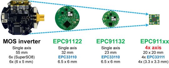
In motor-driven systems, especially in robotics, being able to work at higher switching frequencies has a direct impact on how well the mechanics work and how well the system works together. GaN-based power stages enable finer current control and reduced torque ripple, while also reducing the size of passive filtering components.
From a reliability point of view, using fewer electrolytic capacitors can make a system last longer, especially in mobile or mechanically stressed settings. The trade-off is that you need strong protection and control strategies because switching transients are more sensitive.
Low-voltage GaN allows for higher functional density within limited mechanical envelopes as robotic systems add more actuators and distributed intelligence.

Importance for new automotive electrical architectures
Automotive electrical systems are switching to higher power distribution voltages, and 48 V architectures are becoming more common as a compromise. It's still hard to design a way to quickly and easily switch from 48 V to older voltage levels.
Low-voltage GaN devices lose less power and take up less space in these conversion stages. However, when used in cars, they need to be carefully planned for qualification, long-term reliability, and fault tolerance. The physics of the device itself are good, but system-level validation is still a big part of whether or not it will be widely used.
:quality(80):fill(efefef,0)/p7i.vogel.de/wcms/5f/fe/5ffedb2e0ffa6/listing.jpg)
Design challenges and knowledge requirements
Even though things have gotten better recently, using low-voltage GaN still creates design problems that aren't easy to solve. High dv/dt and di/dt require careful layout control, optimized gate driving, and thorough EMI reduction plans. Also, protection systems must be able to handle quick fault propagation.
As GaN takes over jobs that silicon used to do, engineering discipline and design methodology become just as important as how well the device works. Education, modeling, and application-specific reference designs are very important for making sure that systems behave in a way that can be predicted and repeated.
Conclusion
With the advent of seventh-generation GaN technology, these devices can now be used for low-voltage power conversion. GaN is now able to be utilized in applications below 40 V where efficiency, density, and transient performance are crucial because of advancements in channel resistance, current spreading, and manufacturing consistency.
This development gives engineers a new choice for sophisticated electrical architectures, robotics, and artificial intelligence, but it does not negate silicon's use in low-voltage circuits. The technological viability of GaN in applications that were previously thought to be difficult is confirmed by tangible examples of seventh-generation devices, which exhibit low on-resistance, quick switching, and optimized thermal performance.
(ID:50707852)


:quality(80)/p7i.vogel.de/wcms/7d/b4/7db4fc5b8cd18e6eb2c864a3c329f177/0129545524v2.jpeg)
:quality(80)/p7i.vogel.de/wcms/f5/d2/f5d2bce7c01775fe62d4c6ecebc8c5ba/0129188745v2.jpeg)
:quality(80)/p7i.vogel.de/wcms/cb/38/cb38bf951c0af8a8de423fedce2489d8/0129352475v2.jpeg)
:quality(80)/p7i.vogel.de/wcms/b8/13/b8139abf82c98aa04248a4a119d28c13/0129194616v2.jpeg)
:quality(80)/p7i.vogel.de/wcms/60/40/6040b2e00aef20b4f9d92e8ac9f79c32/0129349725v2.jpeg)
:quality(80)/p7i.vogel.de/wcms/b3/13/b313941dbf7adc57c6d144966106d82b/0129219607v2.jpeg)
:quality(80)/p7i.vogel.de/wcms/56/a4/56a4d9b6ee131a7a00b8b89dabf108f9/0128979281v2.jpeg)
:quality(80)/p7i.vogel.de/wcms/67/62/676279913d77e1db48eb5cbe9be4c767/0128937895v2.jpeg)
:quality(80)/p7i.vogel.de/wcms/d8/18/d8181873ad07a9b0f77c8ef2d82441cb/0129407783v2.jpeg)
:quality(80)/p7i.vogel.de/wcms/f0/d8/f0d82f06ed1b7abb3245dfc4c317cb55/0127949994v2.jpeg)
:quality(80)/p7i.vogel.de/wcms/6e/e5/6ee5ad1dc45fd69a5a5718147605850a/0129347492v2.jpeg)
:quality(80)/p7i.vogel.de/wcms/7d/40/7d406bd959b3a9127c33a66157f9030a/0128339184v4.jpeg)
:quality(80)/p7i.vogel.de/wcms/23/ee/23ee4a97790d6009dbfd7d9577ffa723/0129220424v2.jpeg)
:quality(80)/p7i.vogel.de/wcms/3c/d1/3cd1cacbceb792ba63727199c61ca434/0127801860v2.jpeg)
:quality(80)/p7i.vogel.de/wcms/5a/a0/5aa0436498af618297961fd54ab36cdf/0126290792v2.jpeg)
:quality(80)/p7i.vogel.de/wcms/cb/30/cb30ebdca7fcaea281749cb396654eb3/0124716339v2.jpeg)
:quality(80)/thumbor.vogel.de/kNr3yG3hu6lnpJYlKwKfoOwkLA4=/500x500/p7i.vogel.de/wcms/69/79/6979e4b5bc84c/maurizio-dpe.jpeg)
:fill(fff,0)/p7i.vogel.de/companies/60/7e/607ec89d5d9b5/white-frame.jpg)
:fill(fff,0)/p7i.vogel.de/companies/5f/71/5f71d5f92a5f6/2000px-rogers-corporation-logo-svg.png)
:fill(fff,0)/p7i.vogel.de/companies/68/00/6800eb0040fb9/cobalt-vertical-aligned-bold.png)
:quality(80)/p7i.vogel.de/wcms/0e/13/0e132310ca94e4d27cfc167cbcf567f9/0128546543v2.jpeg)
:quality(80)/p7i.vogel.de/wcms/1b/91/1b91858c324468e86c68b8fdc790864d/0125590741v2.jpeg)