TECHNOLOGY COMPUTER-AIDED DESIGN Optimization of wide bandgap semiconductors through TCAD simulations
Related Vendors
“TCAD” is done before manufacturing wide bandgap (WBG) semiconductors. This article details the role of TCAD simulations in designing efficient WBG semiconductors and discusses the development challenges, future scope, and a case study.

What is TCAD?
Technology Computer-Aided Design (TCAD') is a set of computer simulations to design, develop, optimize, and test the manufacturing processes and operation of real-world physical semiconductors in advance. TCAD performs simulations of semiconductor manufacturing processes and the target manufactured device on a computer. In simple words, TCAD showcases the effect of all semiconductor manufacturing processes in each stage and the performance of assembled target devices through simulations.
TCAD is categorized into a branch of EDA (Electronic Design Automation). Just like any other EDA tool, TCAD is done on software before the actual manufacturing procedure initiates. TCAD is implemented in the R&D departments of semiconductor manufacturing companies. The end result of a TCAD implementation is to generate files and data that ensure the reliability of fabrication procedures and the target device to be manufactured.
Development challenges: What’s the problem with WBG semiconductors?

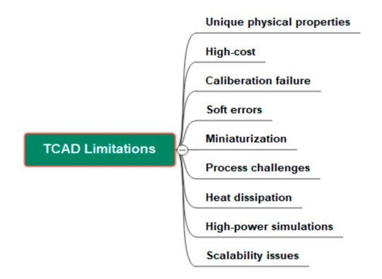
Unique physical properties
Maintaining semiconducting behavior at wider band gaps is tough. These types of materials are at risk of turning into insulators- requiring extra precision, advanced fabrication, and cutting-edge technology.
High-cost
The physical and mechanical conditions required to manufacture WBG require extreme temperatures, pressures, radiations, magnetic fields, and a controlled environment. Introducing such physical conditions increases the costs associated with each manufacturing stage.
Calibration failure
A variation occurs in selecting the appropriate physical model, describing the processes, defining the boundary conditions, and adjusting the parameters. Certain circuit patterning processes are physically too dependent upon equipment.
Soft errors
TCAD Simulations tend to face “soft errors” in various VLSI design styles. A soft error is an unexpected signal variation caused by a chemical reaction, defect in lattice, or noise.
:quality(80)/p7i.vogel.de/wcms/65/60/6560ef5e57a2190a5bc11052d71fe13e/95589268.jpeg)
ELECTRONIC DESIGN AUTOMATION
The evolution of electronic design automation technology
Miniaturization
TCAD faces challenges in the manufacturing of WBG transistors at high levels of miniaturization. The problem lies in identifying suitable architecture of operational transistors at or below the 3 nm process.
Process challenges
TCAD often incurs challenges based on the semiconductor circuit design stage of photolithography and etching. Furthermore, eliminating defects in the doping and diffusion stage is critical to TCAD's success.
Heat dissipation
WBG semiconductors, especially SiC and GaN in high-power applications, require thermal management systems. TCAD simulations determine the DC/AC characteristics of WBG semiconductors. Engineers optimize the design and choose appropriate packaging for heat and losses.
High-power simulations
The inability to predict the accurate behavior of high-power WBG semiconductors is an industry-wide problem. TCAD simulations are tougher for kilo volts and currents above hundred amperes.
Scalability issues
Limited TCAD data is available to verify and confirm the accuracy of WBG simulations, compared to traditional Si models. Exceptional engineering input is required to solve design and reliability challenges.
The role of TCAD simulations
A variety of TCAD tools are available in the market for performing simulations at each stage of the semiconductor design flow and for the end device. Most TCAD tools implement GUI, ML, AI, and various other advanced technologies. The collaborative environment offers processing and management of simulations. The best possible way to access the full benefits of TCAD is to opt for the TCAD software suite or package. The role of TCAD in developing WBG semiconductors is listed below.

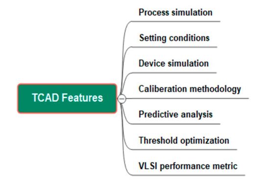
Process simulation
TCAD typically performs simulations for front-end semiconductor manufacturing processes like wafer processing, photolithography, logic circuit design, etching, doping, diffusion, etc. TCAD also tests the behavior of semiconductors in back-end processes like assemblies and packages under different physical and electrical conditions.
Setting conditions
TCAD simulation starts with a defined geometry of the initial structure and mesh. Engineers define process steps and sequences with the description of virtual equipment. Analytical rate, Monte Carlo analysis, string algorithms, and nonlinear least square optimization are some methods.
Device simulation
The data from the process simulation is the input for the target device simulation. TCAD performs compact modeling for DUT (Device Under Test). TCAD offers simulations under various quantum, physical, mechanical, thermal, electrical, optical, and boundary conditions.
Calibration methodology
TCAD simulators must be calibrated to match real-time experiments. Calibrated physical models enable fabs to virtually analyze manufacturing processes and costs. Calibration implements statistical analysis to remove soft error vulnerabilities and variation between simulations and available experimental data.
Predictive analysis
TCAD simulations provide simulations with fewer errors for various WBG semiconductors. Simulations run on an atomic scale to predict the behavior of lattice imperfections, nuclear reactions, tunneling, ballistic transport, and DC/AC characteristics. Even parasitic effects are studied through interconnect simulations.
Threshold optimization
WBG semiconductors used for ultra-low power applications are susceptible to variations in manufacturing processes. TCAD performs simulations to understand the level of sensitivity, device performance, and power consumption. The reliability analysis can optimize the threshold operation of WBG semiconductors.
VLSI performance metric
TCAD shortens the VLSI design cycle for logic integration. Low-power WBG semiconductors tend to have a reduced VLSI design cycle through TCAD simulations. According to a 2016 study, TCAD results in reducing 40% development cost.
:quality(80)/p7i.vogel.de/wcms/20/71/207153e4519e1794b37888a955982422/88807673.jpeg)
AI
The impact of artificial intelligence on the semiconductor industry
Case study
The recent TCAD case study is Fraunhofer IISB’s solutions to Silicon-on-Insulator Tunnelling Field Effect Transistor (SoI TFET).
TFET (Tunneling Field Effect Transistor) is a suitable device for low-power applications. More experimental data is needed to determine the appropriate physical model and functionality of TFETs. TFETs use quantum tunneling to operate compared to traditional carrier injection methods. Quantum tunneling is talked about in our Zener diode and Schottky diode articles. In simple words, quantum tunneling is the phenomenon where electrons cross an impossible energy barrier through a “tunnel” from one side to another.
Fraunhofer IISB showcases three tunneling band-to-band paths. The first one, direct tunneling (DT), is a conventional method in which an electron tunnels from the valence band to the conduction band. The second method is phonon-assisted tunneling (PAT) where lattice vibration enables quantum tunneling in between bands. At last, trap-assisted tunneling (TAT) is possible through localized states that tunnel from one band to the other on the opposite side of the barrier but within the energy band gap.
The processes were set in TCAD with values like gate length, doping profile, thickness, etc, for SoI TFET. The procedure ran simulations on various models and calibrated parameters for each tunneling path. The comparison to experimental data reproduced variations of output characteristics under several conditions. In conclusion, the case study generated relevant results for SoI TFET that can be crucial for manufacturing and understanding device performance.
:quality(80):fill(efefef,0)/p7i.vogel.de/wcms/5f/fe/5ffedb2e0ffa6/listing.jpg)
Future perspectives
In the case of WBG semiconductors, TCAD tends to optimize physical properties and reduce fabrication costs. TCAD is empowering Moore’s law through WBG semiconductor optimization that may result in further miniaturization. The time-to-market acceleration of WBG semiconductors leads to improved efficiency, performance, and reliability in applications such as power electronics, renewable energy, and electric vehicles.
Conclusion
TCAD is a useful software-based technology for estimating the results of manufacturing processes at each stage and determining the properties of manufactured WBG semiconductors. TCAD provides a simulation of each process in semiconductor fabrication: ranging from epitaxial growth of crystals, wafer processing, logic circuit design, photolithography, patterning, and dopant implantation to interconnect modeling.
Even after the simulation of manufacturing and packaging processes, TCAD enables analyzing the functionality, improving efficiency and optimization of target semiconductors. Simply put, TCAD is a way to experiment with what is right and what is not to save time for fabs from directly starting wafer processing. TCAD can help engineers prepare “data sheets in advance” before manufacturing initiates on a bare wafer!
References
- https://ieeexplore.ieee.org/document/9592554
- https://publica-rest.fraunhofer.de/server/api/core/bitstreams/fbfe84cc-4a40-41f6-848e-1866a1ea465b/content
Power Electronics in the Energy Transition

The parameters for energy transition and climate protection solutions span education, research, industry, and society. In the new episode of "Sound On. Power On.", Frank Osterwald of the Society for Energy and Climate Protection Schleswig‐Holstein talks about the holistic guidance his organization can provide.
Listen now!
(ID:49964884)


:quality(80)/p7i.vogel.de/wcms/2f/f3/2ff3221bf7665de2d0acf83760bfd1fa/0130031523v2.jpeg)
:quality(80)/p7i.vogel.de/wcms/c3/16/c316e955a97f5d72d9678297b237b9e5/0129932858v2.jpeg)
:quality(80)/p7i.vogel.de/wcms/ef/0a/ef0adb0acf793fe147cc27c21f6a7a67/0129954238v2.jpeg)
:quality(80)/p7i.vogel.de/wcms/53/f9/53f9301dfc9292d02960f7996c79cc6e/0129927601v2.jpeg)
:quality(80)/p7i.vogel.de/wcms/6e/cd/6ecd41d095d5111cf4ed37b714844487/0129930878v2.jpeg)
:quality(80)/p7i.vogel.de/wcms/02/c0/02c0e9722f70b1134dbf96fb59a9c73d/0129655179v2.jpeg)
:quality(80)/p7i.vogel.de/wcms/cc/67/cc670ea2029cd2af5c641af70e1bf734/0129816392v4.jpeg)
:quality(80)/p7i.vogel.de/wcms/ea/e6/eae6aee30071e67a5627027974437134/0129544613v2.jpeg)
:quality(80)/p7i.vogel.de/wcms/b1/5e/b15ee02b0ba02db70cf61e37d66ad1d3/0129349127v2.jpeg)
:quality(80)/p7i.vogel.de/wcms/26/d5/26d591cc340077026eac56a0e7564faf/0129949603v2.jpeg)
:quality(80)/p7i.vogel.de/wcms/4d/e0/4de02f76a37cbb3df30dd231de589c8e/0128866890v2.jpeg)
:quality(80)/p7i.vogel.de/wcms/18/0b/180b7b63afc91e523592d8a5ce161c96/0129847487v2.jpeg)
:quality(80)/p7i.vogel.de/wcms/be/c8/bec8d43fc0ee73414274be44608b2970/0129748903v2.jpeg)
:quality(80)/p7i.vogel.de/wcms/23/ee/23ee4a97790d6009dbfd7d9577ffa723/0129220424v2.jpeg)
:quality(80)/p7i.vogel.de/wcms/3c/d1/3cd1cacbceb792ba63727199c61ca434/0127801860v2.jpeg)
:quality(80)/p7i.vogel.de/wcms/5a/a0/5aa0436498af618297961fd54ab36cdf/0126290792v2.jpeg)
:fill(fff,0)/p7i.vogel.de/companies/60/7e/607ec89d5d9b5/white-frame.jpg)
:fill(fff,0)/p7i.vogel.de/companies/66/8b/668becd1c07eb/dowa-logo-word--1-.jpeg)
:fill(fff,0)/p7i.vogel.de/companies/69/30/693022b11e5db/logo.jpeg)
:quality(80)/p7i.vogel.de/wcms/0e/13/0e132310ca94e4d27cfc167cbcf567f9/0128546543v2.jpeg)
:quality(80)/p7i.vogel.de/wcms/7b/2c/7b2c4ddd6c8fd3b44fe8afc18f0d7e40/0115676667.jpeg)