SEMICONDUCTORS China's non-silicon transistor redefines speed in semiconductors
Related Vendors
China invented the fastest transistor in the world, and it is not made from silicon. Surprisingly, the quickest semiconductor was never known to be a semiconductor. It is not even a metal! The fastest transistor runs 40 % faster than Intel's and TSMC's famous processors. Check out the story to learn about the latest “fastest transistor” news coming from the semiconductor industry. Maybe it could open the door for us to live in the “silicon-less world”.

While the semiconductor fabrication industry looks forward to 2-nm and 1-nm chips, an unexpected invention took place in China. Despite facing trade tensions with the US, China went on to invent the world’s fastest transistor. Peking University, based in Beijing, invented a transistor built on the foundation of the Bismuth compound, a typical semiconductor. The inventors hail, “It is the fastest, most efficient transistor ever”. The fastest transistor is reported to consume 10 % of the power compared to today’s chips.
Silicon-free transistor
Silicon, of course, the most abundant and cheapest material for building transistors, remains hard to replace. The semiconductor industry is keen to find silicon alternatives as we might eventually run out of silicon. In addition, we need more efficiency than what silicon offers. The new transistor is surprisingly not made from Silicon. Bismuth, another chemical element in the periodic table, is the “building 2D material”.
Bismuth bonus
Bismuth, as an element, is not a semiconductor. It exhibits an electrical conductivity of 77,000 S/m. Semiconductors must have a band gap. In metals, energy bands overlap for conduction. In Bismuth, a slight band gap exists between its energy bands— making it rather a “semimetal”.
Scientists used Bismuth Oxyselenide as the main semiconducting material to create the conductive channel. It is a ternary compound of Bismuth (Z = 83), Oxygen (Z = 8), and Selenium (Z = 34). Another oxide from the same three elements, Bismuth Selenite Oxide, was used to create the gate dielectric.
:quality(80):fill(efefef,0)/p7i.vogel.de/wcms/5f/fe/5ffedb2e0ffa6/listing.jpg)
Bismuth as GAA FET
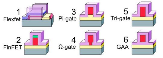
Bismuth oxyselenide formed a GAA transistor (Gate-all-around transistor). GAA is an advanced transistor architecture in which the gate covers the entire channel on all four sides. It is the successor of FinFET, another legacy transistor architecture known for its miniaturization capabilities. GAA further boosts miniaturization and low-power designs.

The image above shows multigate transistor models. In FinFET, a green-colored ‘fin’, made using silicon, acts like a channel. The purple-colored gate wraps around three sides of the fin. In GAA, the purple-colored gate covers the entire red-colored channel from all dimensions.
2D structure: Something new?
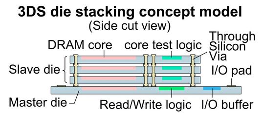
Semiconductors exhibit either 3D or 2D structures. 3D semiconductors are stacked on a single substrate. These are traditional structures where semiconductors are interconnected vertically. The master-slave diagram below explains 3D semiconductors through a chip-on-chip structure!

The inventors consider that 2D transistors are capable of “changing lanes” in the semiconductor world. Graphene is a promising example of a 2D semiconductor. In fact, 2D heterostructures support miniaturization and quantum applications.

In 2D semiconductors, atoms are confined to have thickness only in two dimensions. They are arranged in thin layers, like a sheet. As a result, 2D semiconductors are atomically ultra-thin and show reduced leakage current and power consumption.
Experiment went on like this…
Ultra-thin sheets of bismuth oxyselenide were stacked on the same substrate. Insulating bismuth selenite oxide was applied as a gate dielectric to isolate these thin layers. Multiple such structures were fabricated above the previous ones and linked through interconnects.
Scaling 2D GAA heterostructures remains a challenge in the industry. Bismuth oxyselenide underwent low-temperature monolithic three-dimensional integration. The vertically stacked layers of bismuth oxyselenide were fabricated on a single substrate at low temperatures to prevent base layer damage.
Groundbreaking results
A 2D Bismuth Oxyselenide GAA transistor was manufactured with a 30 nm gate length. The new transistor showcased exceptional properties such as:
| Observation Parameter | Value |
| Electron Mobility | 280 cm2/Vs |
| Subthreshold Swing | 62 mV/dec |
| Operation Voltage | 0.5 V |
| On-state Current | >1 mA/m |
| Intrinsic Delay | 1.9 picosecond |
| Energy-delay Product | 280 cm2/Vs |
The main advantage is its efficient operation compared to silicon. A higher dielectric constant of the gate material helps to hold and control charges more efficiently. The researchers compare the current flow in the fastest transistor to the smooth water flow in a pipe.
The 3-nm FinFETs have an intrinsic delay of about 0.43 seconds. With a delay of just 1.9 picoseconds, bismuth oxyselenide becomes the fastest transistor, capable of operating in the sub-terahertz frequency range.
Transistor so fast, you can’t imagine
The fastest devices, so far, were operational in Gigahertz. Gigahertz frequencies are what WiFi networks and Bluetooth devices operate at. Terahertz frequencies are applicable in advanced scanning, medical imaging, and research.
A human heart beats 100,000 times a day, roughly 3 billion times per year. A Terahertz device is capable of switching 1,000,000,000,000 times per second! No such biological system operates that fast. In simple words, you can consider Terahertz frequencies as big as a trillion!
What innovation does the fastest transistor bring?
China is battling the semiconductor monopoly of the West through innovations like DeepSeek AI and now this— the fastest transistor. Continuous pressure to eliminate silicon and build homemade chips is driving the country towards such steps. The inventing team is already working on scaling the production.
Reliable mature nodes
With a gate length of 30 nm, bismuth oxyselenide falls into the category of mature process nodes. Small chips, about 7 nm, have a gate length of 20 nm. At present, 3 nm chips have a gate length between 12 to 14 nm. With a 30 nm gate length in a 2D GAA heterostructure, bismuth selenide can be applicable in 28 nm and 65 nm chips.
:quality(80)/images.vogel.de/vogelonline/bdb/1722500/1722532/original.jpg)
Interview
From quantum sensors to quantum computers
1-nanometer chips
Due to its 2D structure and GAA model, Bismuth oxyselenide has a huge potential for reaching the 1 nm mode in the future. 2D structures are what quantum technology bets on. Inventors quote “This work demonstrates that 2D GAAFETs do exhibit comparable performance and energy efficiency to commercial silicon-based transistors, making them a promising candidate for the next technology node.”
Power electronics
High electron mobility and faster switching make the transistor applicable in a variety of optoelectronic, RF power, and microwave applications. A low operating voltage of 0.5 V enables bismuth oxyselenide to achieve a faster and more sustained performance without overheating. Consuming 10 % less energy is a high number in maintaining power budgets. As a result, the latest fastest transistor could someday solve the power consumption and overheating problem in power electronics.
References
PCIM Expo 2026: Join the leading exhibition!

Lead the future of power electronics! Exhibit your latest solutions, connect with key players, and elevate your brand visibility worldwide at the PCIM Expo from 9 – 11 June 2026 in Nuremberg, Germany. Benefit from our Early Bird discount by 30 June 2025.
Secure your spot now
(ID:50466377)


:quality(80)/p7i.vogel.de/wcms/2f/f3/2ff3221bf7665de2d0acf83760bfd1fa/0130031523v2.jpeg)
:quality(80)/p7i.vogel.de/wcms/c3/16/c316e955a97f5d72d9678297b237b9e5/0129932858v2.jpeg)
:quality(80)/p7i.vogel.de/wcms/ef/0a/ef0adb0acf793fe147cc27c21f6a7a67/0129954238v2.jpeg)
:quality(80)/p7i.vogel.de/wcms/53/f9/53f9301dfc9292d02960f7996c79cc6e/0129927601v2.jpeg)
:quality(80)/p7i.vogel.de/wcms/6e/cd/6ecd41d095d5111cf4ed37b714844487/0129930878v2.jpeg)
:quality(80)/p7i.vogel.de/wcms/02/c0/02c0e9722f70b1134dbf96fb59a9c73d/0129655179v2.jpeg)
:quality(80)/p7i.vogel.de/wcms/cc/67/cc670ea2029cd2af5c641af70e1bf734/0129816392v4.jpeg)
:quality(80)/p7i.vogel.de/wcms/ea/e6/eae6aee30071e67a5627027974437134/0129544613v2.jpeg)
:quality(80)/p7i.vogel.de/wcms/b1/5e/b15ee02b0ba02db70cf61e37d66ad1d3/0129349127v2.jpeg)
:quality(80)/p7i.vogel.de/wcms/26/d5/26d591cc340077026eac56a0e7564faf/0129949603v2.jpeg)
:quality(80)/p7i.vogel.de/wcms/4d/e0/4de02f76a37cbb3df30dd231de589c8e/0128866890v2.jpeg)
:quality(80)/p7i.vogel.de/wcms/18/0b/180b7b63afc91e523592d8a5ce161c96/0129847487v2.jpeg)
:quality(80)/p7i.vogel.de/wcms/be/c8/bec8d43fc0ee73414274be44608b2970/0129748903v2.jpeg)
:quality(80)/p7i.vogel.de/wcms/23/ee/23ee4a97790d6009dbfd7d9577ffa723/0129220424v2.jpeg)
:quality(80)/p7i.vogel.de/wcms/3c/d1/3cd1cacbceb792ba63727199c61ca434/0127801860v2.jpeg)
:quality(80)/p7i.vogel.de/wcms/5a/a0/5aa0436498af618297961fd54ab36cdf/0126290792v2.jpeg)
:fill(fff,0)/p7i.vogel.de/companies/5f/71/5f71d5f92a5f6/2000px-rogers-corporation-logo-svg.png)
:fill(fff,0)/p7i.vogel.de/companies/66/9a/669a2816c84be/pcim-logo.png)
:fill(fff,0)/p7i.vogel.de/companies/66/8b/668becd1c07eb/dowa-logo-word--1-.jpeg)
:quality(80)/p7i.vogel.de/wcms/b9/18/b918d8d0e447a18f7b9e983c25b96330/0125855402v2.jpeg)
:quality(80)/p7i.vogel.de/wcms/0c/71/0c7136f0406689ac88a83b3d5c9404c8/0123816960v2.jpeg)