ARTIFICIAL INTELLIGENCE AI-powered depth profiling: Revolutionizing SiC MOSFET analysis
Related Vendors
While exploring the benefits of 3D SIMS imaging for SiC MOSFET analysis, the discussion acknowledges its time-consuming nature and introduces a machine learning approach that achieves 95 % accuracy in defect identification. This innovation reduces analysis time from thousands of hours to just days, highlighting AI's transformative potential in power electronics research.

In my previous article I talked about the need for 3D SIMS imaging. This is not always the case, as simple, fast-depth profiling can provide sufficiently good results. Nonetheless three-dimensional SIMS imaging will always provide the most detailed and accurate results, revealing fine structural and compositional details. However, it has one undeniable drawback: it is time-consuming and requires significant preparation. Time is money and often we just need an answer fast.

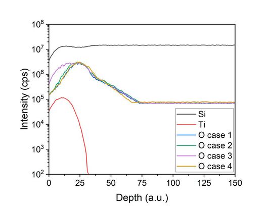
Let's have a look at Figure 1, which shows a depth profile of a simple SiC MOSFET transistor. Although this is a planar structure, the metallic contacts and gate oxide protrude above the semiconductor surface, causing slight signal broadening in the final depth profile.
There are overlaid oxygen measurements for four different structures in the figure. It is difficult to differentiate which example represents the functioning device and which suffers from oxygen contamination.
Aside from the good case, there is one in which oxygen has infiltrated the metal-semiconductor interface, another where a high oxygen content is found in the metallization, and yet another where oxygen is present in the semiconductor itself. Note that the differences are very subtle. The most apparent case is the third one, where oxygen contamination in the metal is evident. It becomes difficult when multiple areas are affected, there would be no way to differentiate these situations using only simple depth profiles.
:quality(80)/p7i.vogel.de/wcms/20/71/207153e4519e1794b37888a955982422/88807673.jpeg)
AI
The impact of artificial intelligence on the semiconductor industry
We can leverage machine learning to solve this problem. By training a system on dozens, or better yet, hundreds of depth profiles corresponding to different cases, it can learn to recognize real-world profiles and provide accurate assessments. John J. Hopfield and Geoffrey Hinton were awarded the Nobel Prize in Physics 2024 “for foundational discoveries and inventions that enable machine learning with artificial neural networks."
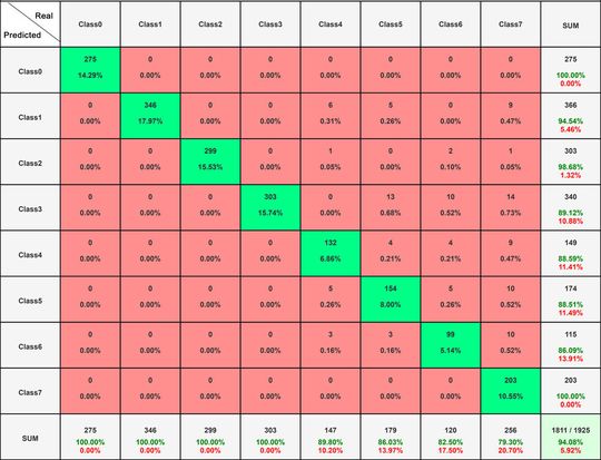
Look at the confusion matrix below:

Not once was a good structure classified as defective or vice versa. The only minor shortcomings arise when the system occasionally indicates more defects than actually exist in a given device. However, this is a relatively small limitation. Moreover, for nearly 2,000 depth profiles, the prediction accuracy was close to 95 %.
But what makes this even more interesting is that it only took 4 days to perform 2,000 depth profiles. The same amount of 3D SIMS images would take almost 10,000 hours, which is over a year.
It is just one example of how AI can revolutionize power electronics research. Machine learning can be applied not only to depth profiling analysis but also to failure detection, process optimization, material characterization, and predictive maintenance.
PCIM Expo 2025: Join the industry highlight

Position your company at the forefront of the power electronics industry! Exhibit at the PCIM Expo 2025 in Nuremberg, Germany to showcase your solutions and connect with top decision-makers and innovators driving the industry forward.
Learn more
(ID:50358249)


:quality(80)/p7i.vogel.de/wcms/2f/f3/2ff3221bf7665de2d0acf83760bfd1fa/0130031523v2.jpeg)
:quality(80)/p7i.vogel.de/wcms/c3/16/c316e955a97f5d72d9678297b237b9e5/0129932858v2.jpeg)
:quality(80)/p7i.vogel.de/wcms/ef/0a/ef0adb0acf793fe147cc27c21f6a7a67/0129954238v2.jpeg)
:quality(80)/p7i.vogel.de/wcms/53/f9/53f9301dfc9292d02960f7996c79cc6e/0129927601v2.jpeg)
:quality(80)/p7i.vogel.de/wcms/6e/cd/6ecd41d095d5111cf4ed37b714844487/0129930878v2.jpeg)
:quality(80)/p7i.vogel.de/wcms/02/c0/02c0e9722f70b1134dbf96fb59a9c73d/0129655179v2.jpeg)
:quality(80)/p7i.vogel.de/wcms/cc/67/cc670ea2029cd2af5c641af70e1bf734/0129816392v4.jpeg)
:quality(80)/p7i.vogel.de/wcms/ea/e6/eae6aee30071e67a5627027974437134/0129544613v2.jpeg)
:quality(80)/p7i.vogel.de/wcms/b1/5e/b15ee02b0ba02db70cf61e37d66ad1d3/0129349127v2.jpeg)
:quality(80)/p7i.vogel.de/wcms/26/d5/26d591cc340077026eac56a0e7564faf/0129949603v2.jpeg)
:quality(80)/p7i.vogel.de/wcms/4d/e0/4de02f76a37cbb3df30dd231de589c8e/0128866890v2.jpeg)
:quality(80)/p7i.vogel.de/wcms/18/0b/180b7b63afc91e523592d8a5ce161c96/0129847487v2.jpeg)
:quality(80)/p7i.vogel.de/wcms/be/c8/bec8d43fc0ee73414274be44608b2970/0129748903v2.jpeg)
:quality(80)/p7i.vogel.de/wcms/23/ee/23ee4a97790d6009dbfd7d9577ffa723/0129220424v2.jpeg)
:quality(80)/p7i.vogel.de/wcms/3c/d1/3cd1cacbceb792ba63727199c61ca434/0127801860v2.jpeg)
:quality(80)/p7i.vogel.de/wcms/5a/a0/5aa0436498af618297961fd54ab36cdf/0126290792v2.jpeg)
:quality(80)/thumbor.vogel.de/WdvxZ-fifc7PUi6GumY-je3ivo4=/500x500/p7i.vogel.de/wcms/5f/d9/5fd9c20e33a8f/ppm.jpeg)
:fill(fff,0)/p7i.vogel.de/companies/60/76/607651ea5d461/logo-sq.jpg)
:fill(fff,0)/p7i.vogel.de/companies/66/9a/669a2816c84be/pcim-logo.png)
:fill(fff,0)/p7i.vogel.de/companies/66/8b/668becd1c07eb/dowa-logo-word--1-.jpeg)
:quality(80)/p7i.vogel.de/wcms/77/8a/778aa2874d910b701c3e9aab160aec35/0123969290v2.jpeg)
:quality(80)/p7i.vogel.de/wcms/c2/f1/c2f1acbcc59fdf2cf17b6fe0a7bf7a1d/0125393004v2.jpeg)