DAB CONVERTERS Magnetizing current control in dual-active-bridge converters
Related Vendors
This article explores the control of magnetizing current in Dual Active Bridge (DAB) converters to prevent transformer saturation. Innovative techniques eliminate the need for bulky dc-blocking capacitors, enhancing efficiency and reliability while reducing system costs. The methods presented offer new pathways for optimizing modern power supply systems.

The dual-active-bridge converter or DAB is a popular converter used in charging architectures for electric vehicles (EV). As with any isolated power supply, it is important to keep the transformer magnetic operating point away from saturation in all possible conditions. For this purpose, designers often insert a dc-blocking capacitor in the primary of the transformer to ensure a zeroed average magnetizing current. When used in a bidirectional system, two of these capacitors must be included in the electrical circuit, naturally hampering the size, weight and overall cost of the power supply. Without these additional components, the transformer operating point can shift towards saturation, pushing the converter in a dangerous zone. This article reviews the origins of the issue and gives hints on how to suppress this bulky capacitor when designing a DAB converter.
Watch also the PCIM 2024 TekTalk aboout DAB Converters from Future Electronics:
A bidirectional structure
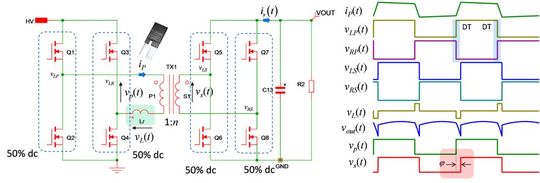
Figure 1 shows the typical configuration of a DAB converter. The primary section is made of a full-bridge whose two legs are operated at a fixed-frequency, 50% duty ratio. They produce an instantaneous voltage vp(t) applied at the primary-side of the transformer. A second full-bridge structure takes place in the secondary side and operates in a similar manner, generating a voltage vs(t). By adjusting the phase shift between the two voltages, primary and secondary, the current circulating in the series inductance Lr is controlled and power flow is adjusted according to the needs. The right-side waveforms illustrate this operating mode with φ the phase shift between the two bridges. Please note a positive shift in this example, implying energy absorbed from the high-voltage input (HV node) and delivered to the resistive load R2. Should the phase shift be negative instead, meaning vs(t) leads vp(t), energy would now come from the secondary-side source to feed a primary-side receptor. The DAB is therefore a bidirectional converter in essence.
Origins of the issue
The primary-side bridge applies the input voltage across the transformer during 50% of the switching period and the opposite level during the rest of the time. Almost all of the primary-side current is scaled to the secondary side via the transformer turns ratio except a small part which circulates as the magnetizing current im. This current cannot be directly measured but you can reconstruct it by combining primary and secondary currents as shown in equation 1:
im(t) = ip(t) - n * is(t)
The magnetizing current drives the transformer operating point and engenders core losses proportional to the flux density swing ΔB observed cycle-by-cycle. The amplitude of this current depends on the magnetizing inductance Lm and the voltage applied at the transformer primary.
In a perfect DAB converter operated at steady state, the transformer magnetizing current is triangular and evolves between a peak and a valley of similar absolute values. The transformer magnetic point therefore operates in quadrants I and III, symmetrically across the x-axis of the B-H curve. If the volt-seconds applied during half of the switching period are equal to the volt-seconds applied with opposite polarity, then the average voltage across the transformer primary is zero, implying a magnetizing current also equal to zero.
The voltage applied across the transformer during switching phases, depends on the various voltage drops and timing values. The voltage drops are linked to the ohmic paths encountered during the switching events among which the rDS(on) of the transistors plays a significant role. This resistance varies from lots to lots but also in temperature. In conjunction with the circulating currents, they affect the voltage delivered at the transformer primary.
Volt-seconds calculation involves a voltage but also a duration. The exact timing of the waveforms is therefore a key contributor for the possible mismatch in the applied volt-seconds. If the internal timer resolution is not small enough or if asymmetrical propagation delays unbalance the on- and off-time lengths, then a shift in the average voltage applied to the transformer primary is inevitable.
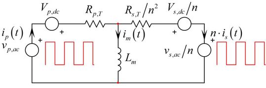
In this drawing, the resistive components Rp and Rs, lump all ohmic losses such as transistors rDS(on) but also PCB copper traces and wires resistance. The series sources Vp,dc and Vs,dc represent the small dc mismatches in the applied averaged voltages which can potentially lead to a shift in the magnetic operating point. Knowing that an efficient design will strive to keep these ohmic drops to a minimum, any small dc offset will end up in a significant average current deviation. It is possible to quantify the shift in flux density as given in equation 2.
With n the transformer turns ratio, Np the primary turns, μ0 and μr are respectively the permeability of free space and the permeability of the magnetic material and finally, lm represents the mean magnetic path length of the adopted core.
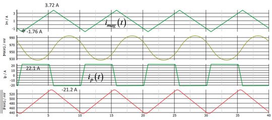
A quick simulation of a 12-kW DAB shown in Figure 3 confirms a shift in the magnetizing current but also in the transformer primary and secondary windings. The observation of the magnetizing current waveform shows different positive and negative peak values, leading to an average level of 930 mA. It is a significant number, potentially pushing the operating point closer to the saturation level with associated distortion in the waveforms. On top of this value, the primary winding exhibits a shift of 483 mA which reaches –800 mA for the secondary side. These offsets affect the circulating rms currents and will increase conduction losses in the semiconductors in both sides of the transformer.
What are the solutions?
Reference [1] reviews the many possible options to monitor the circulating currents and limit the dc shifts. These options include passive and active circuits, starting from gapping the core to active flux control. Active flux control is actually a solution explored in [2] and implemented with digital control. It consists of reconstructing the magnetizing current and slightly modulating the primary and secondary waveforms to keep this current to zero on average. The technique also offers a way to reduce the offset in the currents circulating in the primary and secondary windings.
For simulation purposes, the two inner loops are implemented in an analogue way as shown in Figure 4. The primary and secondary currents are sensed via current transformers then scaled and subtracted for delivering the magnetizing current. A low-ripple averaged value is then treated via a dedicated modulator which acts upon the applied duty ratio of the secondary-side control waveforms. This is a fast-reacting loop which takes control during the start-up sequence and transient conditions and ensures a zeroed average magnetizing current at steady state.
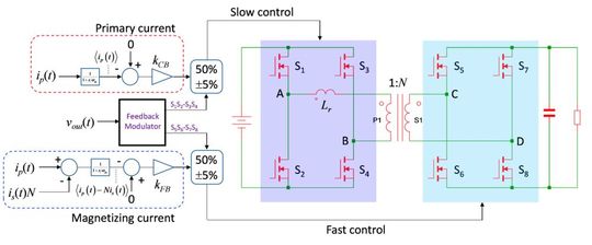
A second loop observes the primary current alone and drives the switching timings to keep the current close to zero on average. This loop is designed with a bandwidth lower than the one taking care of the magnetizing current so as to limit the interaction between the two. For stabilizing the two loops, it is necessary to extract their control-to-output transfer function but this is not a difficult exercise as detailed in [3]. With these expressions in hand, the large low-frequency gain authorizes a simple compensation strategy made of a proportional term only: the goal is not to exactly zero the average currents but to keep their dc drift at minimum values at steady state and under control during transient events.
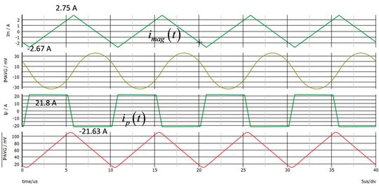
As illustrated in Figure 5, the DAB circuit has been simulated with the two loops turned on. The effects on the currents are immediately visible: the average magnetizing current is down to 1.14 mA while the primary-side current with peaks up to 22 A and exhibits a dc offset of 60.5 mA which is extremely low. The secondary current offset establishes to 95 mA with peaks reaching 33 A.
Conclusion
The DAB converter in its simplest form requires the addition of a dc-blocking capacitor to prevent the transformer from saturating. This capacitor can be bulky and costly for a given project. As detailed in this short article, various techniques exist to remove this passive component and ensure safe operation. The two-loop control system I have described was inspired by a digitally-controlled DAB project and has shown encouraging results, paving the way for the removal of the series capacitor.
Reference
- 1. G. Ortiz et al., Flux Balancing of Isolation Transformers and Application of the “Magnetic Ear” for Closed-Loop Volt-Second Compensation, IEEE Transactions on Power Electronics, Vol. 29, issue 8, August 2014
- 2. M. Jovanović et al., Novel Transformer-Flux-Balancing Control of Dual-Active-Bridge Birectionnal Converters, APEC, March 2015
- 3. C. Basso, Current and Flux Balancing for the Dual Active Bridge Converter, online presentation, 2023
(ID:50072029)


:quality(80)/p7i.vogel.de/wcms/2f/f3/2ff3221bf7665de2d0acf83760bfd1fa/0130031523v2.jpeg)
:quality(80)/p7i.vogel.de/wcms/c3/16/c316e955a97f5d72d9678297b237b9e5/0129932858v2.jpeg)
:quality(80)/p7i.vogel.de/wcms/ef/0a/ef0adb0acf793fe147cc27c21f6a7a67/0129954238v2.jpeg)
:quality(80)/p7i.vogel.de/wcms/53/f9/53f9301dfc9292d02960f7996c79cc6e/0129927601v2.jpeg)
:quality(80)/p7i.vogel.de/wcms/6e/cd/6ecd41d095d5111cf4ed37b714844487/0129930878v2.jpeg)
:quality(80)/p7i.vogel.de/wcms/02/c0/02c0e9722f70b1134dbf96fb59a9c73d/0129655179v2.jpeg)
:quality(80)/p7i.vogel.de/wcms/cc/67/cc670ea2029cd2af5c641af70e1bf734/0129816392v4.jpeg)
:quality(80)/p7i.vogel.de/wcms/ea/e6/eae6aee30071e67a5627027974437134/0129544613v2.jpeg)
:quality(80)/p7i.vogel.de/wcms/b1/5e/b15ee02b0ba02db70cf61e37d66ad1d3/0129349127v2.jpeg)
:quality(80)/p7i.vogel.de/wcms/26/d5/26d591cc340077026eac56a0e7564faf/0129949603v2.jpeg)
:quality(80)/p7i.vogel.de/wcms/4d/e0/4de02f76a37cbb3df30dd231de589c8e/0128866890v2.jpeg)
:quality(80)/p7i.vogel.de/wcms/18/0b/180b7b63afc91e523592d8a5ce161c96/0129847487v2.jpeg)
:quality(80)/p7i.vogel.de/wcms/be/c8/bec8d43fc0ee73414274be44608b2970/0129748903v2.jpeg)
:quality(80)/p7i.vogel.de/wcms/23/ee/23ee4a97790d6009dbfd7d9577ffa723/0129220424v2.jpeg)
:quality(80)/p7i.vogel.de/wcms/3c/d1/3cd1cacbceb792ba63727199c61ca434/0127801860v2.jpeg)
:quality(80)/p7i.vogel.de/wcms/5a/a0/5aa0436498af618297961fd54ab36cdf/0126290792v2.jpeg)
:quality(80)/thumbor.vogel.de/mguFAwuAxCGw9kVi3c_k2-HNi5I=/500x500/p7i.vogel.de/wcms/66/74/667444027a724/tof1.jpeg)
:fill(fff,0)/p7i.vogel.de/companies/62/a0/62a0a0de7d56a/aic-europe-logo.jpeg)
:fill(fff,0)/p7i.vogel.de/companies/66/9a/669a2816c84be/pcim-logo.png)
:fill(fff,0)/p7i.vogel.de/companies/68/08/6808a2b3b6595/het-logo.jpeg)

:quality(80)/p7i.vogel.de/wcms/8c/1a/8c1a6f87a2af9653a5df2d5d963915c0/0118206891v2.jpeg)
:quality(80)/p7i.vogel.de/wcms/7a/a5/7aa50649486f059b1d7111f508c5c6e7/0128629162v2.jpeg)